JAJSEH5C January   2018  – December 2023 DRV5055

PRODUCTION DATA  

  1.   1
  2. 特長
  3. アプリケーション
  4. 概要
  5. Pin Configuration and Functions
  6. Specifications
    1. 5.1 Absolute Maximum Ratings
    2. 5.2 ESD Ratings
    3. 5.3 Recommended Operating Conditions
    4. 5.4 Thermal Information
    5. 5.5 Electrical Characteristics
    6. 5.6 Magnetic Characteristics
    7. 5.7 Typical Characteristics
  7. Detailed Description
    1. 6.1 Overview
    2. 6.2 Functional Block Diagram
    3. 6.3 Feature Description
      1. 6.3.1 Magnetic Flux Direction
      2. 6.3.2 Magnetic Response
      3. 6.3.3 Sensitivity Linearity
      4. 6.3.4 Ratiometric Architecture
      5. 6.3.5 Operating VCC Ranges
      6. 6.3.6 Sensitivity Temperature Compensation for Magnets
      7. 6.3.7 Power-On Time
      8. 6.3.8 Hall Element Location
    4. 6.4 Device Functional Modes
  8. Application and Implementation
    1. 7.1 Application Information
      1. 7.1.1 Selecting the Sensitivity Option
      2. 7.1.2 Temperature Compensation for Magnets
      3. 7.1.3 Adding a Low-Pass Filter
      4. 7.1.4 Designing for Wire Break Detection
    2. 7.2 Typical Application
      1. 7.2.1 Design Requirements
      2. 7.2.2 Detailed Design Procedure
      3. 7.2.3 Application Curve
    3. 7.3 Best Design Practices
    4. 7.4 Power Supply Recommendations
    5. 7.5 Layout
      1. 7.5.1 Layout Guidelines
      2. 7.5.2 Layout Examples
  9. Device and Documentation Support
    1. 8.1 Documentation Support
      1. 8.1.1 Related Documentation
    2. 8.2 ドキュメントの更新通知を受け取る方法
    3. 8.3 サポート・リソース
    4. 8.4 Trademarks
    5. 8.5 静電気放電に関する注意事項
    6. 8.6 用語集
  10. Revision History
  11. 10Mechanical, Packaging, and Orderable Information

パッケージ・オプション

メカニカル・データ(パッケージ|ピン)
サーマルパッド・メカニカル・データ
発注情報

Pin Configuration and Functions

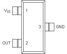
GUID-9E258E76-4C7B-4E1C-832D-D71CAE8A2488-low.gifFigure 4-1 DBZ Package3-Pin SOT-23Top View
GUID-AD9AEAB5-A434-4562-854F-0B5CF105FC59-low.gifFigure 4-2 LPG Package3-Pin TO-92Top View
Table 4-1 Pin Functions
PIN I/O DESCRIPTION
NAME SOT-23 TO-92
VCC 1 1 Power supply. TI recommends connecting this pin to a ceramic capacitor to ground with a value of at least 0.01 µF.
OUT 2 3 O Analog output
GND 3 2 Ground reference