SLES242G December   2009  – December 2014 DRV8412

PRODUCTION DATA.  

  1. Features
  2. Applications
  3. Description
    1.     Simplified Application Diagram
  4. Revision History
  5. Pin Configuration and Functions
    1.     Pin Functions
  6. Specifications
    1. 6.1 Absolute Maximum Ratings
    2. 6.2 ESD Ratings
    3. 6.3 Recommended Operating Conditions
    4. 6.4 Thermal Information
    5. 6.5 Package Heat Dissipation Ratings
    6. 6.6 Package Power Deratings (DRV8412)
    7. 6.7 Electrical Characteristics
    8. 6.8 Typical Characteristics
  7. Detailed Description
    1. 7.1 Overview
    2. 7.2 Functional Block Diagram
    3. 7.3 Feature Description
      1. 7.3.1 Error Reporting
      2. 7.3.2 Device Protection System
        1. 7.3.2.1 Bootstrap Capacitor Undervoltage Protection
        2. 7.3.2.2 Overcurrent (OC) Protection
        3. 7.3.2.3 Overtemperature Protection
        4. 7.3.2.4 Undervoltage Protection (UVP) and Power-On Reset (POR)
      3. 7.3.3 Device Reset
    4. 7.4 Device Functional Modes
  8. Application and Implementation
    1. 8.1 Application Information
    2. 8.2 Typical Applications
      1. 8.2.1 Full Bridge Mode Operation
        1. 8.2.1.1 Design Requirements
        2. 8.2.1.2 Detailed Design Procedure
          1. 8.2.1.2.1 Motor Voltage
          2. 8.2.1.2.2 Current Requirement of 12-V Power Supply
          3. 8.2.1.2.3 Voltage of Decoupling Capacitor
          4. 8.2.1.2.4 Overcurrent Threshold
          5. 8.2.1.2.5 Sense Resistor
        3. 8.2.1.3 Application Curves
      2. 8.2.2 Parallel Full Bridge Mode Operation
      3. 8.2.3 Stepper Motor Operation
      4. 8.2.4 TEC Driver
      5. 8.2.5 LED Lighting Driver
  9. Power Supply Recommendations
    1. 9.1 Bulk Capacitance
    2. 9.2 Power Supplies
    3. 9.3 System Power-Up and Power-Down Sequence
      1. 9.3.1 Powering Up
      2. 9.3.2 Powering Down
    4. 9.4 System Design Recommendations
      1. 9.4.1 VREG Pin
      2. 9.4.2 VDD Pin
      3. 9.4.3 OTW Pin
      4. 9.4.4 Mode Select Pin
      5. 9.4.5 Parallel Mode Operation
      6. 9.4.6 TEC Driver Application
  10. 10Layout
    1. 10.1 Layout Guidelines
      1. 10.1.1 PCB Material Recommendation
      2. 10.1.2 Ground Plane
      3. 10.1.3 Decoupling Capacitor
      4. 10.1.4 AGND
    2. 10.2 Layout Example
      1. 10.2.1 Current Shunt Resistor
    3. 10.3 Thermal Considerations
      1. 10.3.1 DRV8412 Thermal Via Design Recommendation
  11. 11Device and Documentation Support
    1. 11.1 Related Links
    2. 11.2 Trademarks
    3. 11.3 Electrostatic Discharge Caution
    4. 11.4 Glossary
  12. 12Mechanical, Packaging, and Orderable Information

パッケージ・オプション

メカニカル・データ(パッケージ|ピン)
サーマルパッド・メカニカル・データ
発注情報

Description

The DRV841x2 are high-performance, integrated dual full-bridge motor driver with an advanced protection system.

Because of the low RDS(on) of the H-Bridge MOSFETs and intelligent gate drive design, the efficiency of these motor drivers can be up to 97%. This high efficiency enables the use of smaller power supplies and heatsinks, and the devices are good candidates for energy-efficient applications.

The DRV841x2 requires two power supplies, one at 12 V for GVDD and VDD, and another up to 50 V for PVDD. The DRV841x2 can operate at up to 500-kHz switching frequency while still maintaining precise control and high efficiency. The devices also have an innovative protection system safeguarding the device against a wide range of fault conditions that could damage the system. These safeguards are short-circuit protection, overcurrent protection, undervoltage protection, and two-stage thermal protection. The DRV841x2 has a current-limiting circuit that prevents device shutdown during load transients such as motor start-up. A programmable overcurrent detector allows adjustable current limit and protection level to meet different motor requirements.

The DRV841x2 has unique independent supply and ground pins for each half-bridge. These pins make it possible to provide current measurement through external shunt resistor and support multiple motors with different power supply voltage requirements.

Device Information(1)

PART NUMBER PACKAGE BODY SIZE (NOM)
DRV8412 HTSSOP (44) 14.00 mm x 6.10 mm
DRV8432 HSSOP (36) 15.90 mm x 11.00 mm
  1. For all available packages, see the orderable addendum at the end of the data sheet.

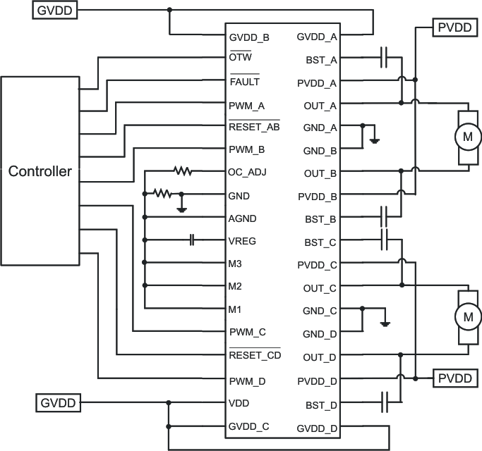
Simplified Application Diagram
DRV8412 DRV8432 fig7_les242.gif