SLVS865J September 2008 – April 2017 DRV8811
PRODUCTION DATA.
- 1 Features
- 2 Applications
- 3 Description
- 4 Revision History
- 5 Pin Configuration and Functions
- 6 Specifications
- 7 Detailed Description
- 8 Application and Implementation
- 9 Power Supply Recommendations
- 10Layout
- 11Device and Documentation Support
- 12Mechanical, Packaging, and Orderable Information
6 Specifications
6.1 Absolute Maximum Ratings
over operating ambient temperature range (unless otherwise noted)(1) (2) (3)| MIN | MAX | UNIT | ||
|---|---|---|---|---|
| Power supply voltage range | VMA, VMB | –0.3 | 40 | V |
| Power supply voltage range | VCC | –0.3 | 7 | V |
| Digital pin voltage range | VI: DIR, DECAY, ENABLEn, HOME, RCA, RCB, RESETn, SLEEPn, SRn, STEP, USM0, USM1 | –0.5 | 7 | V |
| Reference pin voltage range | VREF | –0.3 | 7 | V |
| Sense pin voltage range | ISENA, ISENB(4) | –0.875 | 0.875 | V |
| Output pin voltage range | AOUT1, AOUT2, BOUT1, BOUT2 | –0.7 | VVM + 0.7 | V |
| Gate-drive pin-voltage range | VGD | –0.3 | 8 | V |
| Charge pump pin voltage range | VCP, CP2 | –0.3 | VVM + 12 | V |
| CP1 | –0.3 | VVM | ||
| Peak motor drive output current, IO(peak) | Internally limited | |||
| Operating virtual junction temperature range, TJ | –40 | 150 | °C | |
| Operating ambient temperature range, TA | –40 | 85 | °C | |
| Storage temperature range, Tstg | –60 | 150 | °C | |
(1) Stresses beyond those listed under Absolute Maximum Ratings may cause permanent damage to the device. These are stress ratings only, and do not imply functional operation of the device at these or any other conditions beyond those indicated under Recommended Operating Conditions. Exposure to absolute-maximum-rated conditions for extended periods may affect device reliability.
(2) All voltage values are with respect to network ground terminal.
(3) Power dissipation and thermal limits must be observed.
(4) Transients of ±1 V for less than 25 ns are acceptable.
6.2 ESD Ratings
| VALUE | UNIT | ||||
|---|---|---|---|---|---|
| V(ESD) | Electrostatic discharge | Human body model (HBM), per ANSI/ESDA/JEDEC JS-001(1) | ±2500 | V | |
| Charged device model (CDM), per JEDEC specification JESD22-C101(2) | ±1000 | ||||
(1) JEDEC document JEP155 states that 500-V HBM allows safe manufacturing with a standard ESD control process.
(2) JEDEC document JEP157 states that 250-V CDM allows safe manufacturing with a standard ESD control process.
6.3 Recommended Operating Conditions
over operating ambient temperature range (unless otherwise noted)| MIN | NOM | MAX | UNIT | ||
|---|---|---|---|---|---|
| VVMx | Motor power supply voltage range(1) | 8 | 38 | V | |
| VCC | Logic power supply voltage range | 3 | 5.5 | V | |
| VVREF | VREF input voltage | 0 | VCC | V | |
| RX | RX resistance value | 12 | 56 | 100 | kΩ |
| CX | CX capacitance value | 470 | 680 | 1500 | pF |
(1) Both VMx pins must be connected to the same supply voltage.
6.4 Thermal Information
| THERMAL METRIC(1) | DRV8811 | UNIT | |
|---|---|---|---|
| PWP (HTSSOP) | |||
| 28 PINS | |||
| RθJA | Junction-to-ambient thermal resistance | 31.4 | °C/W |
| RθJC(top) | Junction-to-case (top) thermal resistance | 19.3 | °C/W |
| RθJB | Junction-to-board thermal resistance | 11.5 | °C/W |
| ψJT | Junction-to-top characterization parameter | 0.4 | °C/W |
| ψJB | Junction-to-board characterization parameter | 11.2 | °C/W |
| RθJC(bot) | Junction-to-case (bottom) thermal resistance | 2.8 | °C/W |
(1) For more information about traditional and new thermal metrics, see Semiconductor and IC Package Thermal Metrics.
6.5 Electrical Characteristics
over operating ambient temperature range (unless otherwise noted)| PARAMETER | TEST CONDITIONS | MIN | TYP | MAX | UNIT | |
|---|---|---|---|---|---|---|
| POWER SUPPLIES | ||||||
| IVM | VM operating supply current | VM = 35 V, fPWM < 50 KHz | 4.5 | 8 | mA | |
| IVCC | VCC operating supply current | fPWM < 50 KHz | 0.4 | 4 | mA | |
| IVMQ | VM sleep mode supply current | VM = 35 V | 12 | 20 | μA | |
| IVCCQ | VCC sleep mode supply current | 5 | 20 | μA | ||
| VUVLO | VM undervoltage lockout voltage | VM rising | 6.7 | 8 | V | |
| VCC undervoltage lockout voltage | VCC rising | 2.71 | 2.95 | |||
| VREF INPUT, CURRENT CONTROL ACCURACY | ||||||
| IVREF | VREF input current | VVREF = 3.3 V | –3 | 3 | μA | |
| ΔICHOP | Chopping current accuracy | VVREF = 2 V, 70% to 100% current | –5% | 5% | ||
| VVREF = 2 V, 20% to 56% current | –10% | 10% | ||||
| LOGIC-LEVEL INPUTS | ||||||
| VIL | Input low voltage | 0.3 × VCC | V | |||
| VIH | Input high voltage | 0.7 × VCC | V | |||
| IIL | Input low current | VI = 0.3 × VCC | –20 | 20 | μA | |
| IIH | Input high current | VIN = 0.3 × VCC | –20 | 20 | μA | |
| RPU | Pullup resistance | ENABLEn, RESETn | 1 | MΩ | ||
| RPD | Pulldown resistance | DIR, STEP, SLEEPn, USM1, USM0, SRn | 1 | MΩ | ||
| HOMEn OUTPUT | ||||||
| VOL | Output low voltage | IO = 200 μA | 0.3 × VCC | V | ||
| VOH | Output high voltage | IO = –200 μA | 0.7 × VCC | V | ||
| DECAY INPUT | ||||||
| VIL | Input low threshold voltage | For fast decay mode | 0.21 × VCC | V | ||
| VIH | Input high threshold voltage | For slow decay mode | 0.6 × VCC | V | ||
| H-BRIDGE FETS | ||||||
| rDS(on) | HS FET on resistance | VM = 24 V, IO = 2.5 A, TJ = 25°C | 0.50 | Ω | ||
| VM = 24 V, IO = 2.5 A, TJ = 85°C | 0.60 | 0.75 | ||||
| rDS(on) | LS FET on resistance | VM = 24 V, IO = 2.5 A, TJ = 25°C | 0.50 | Ω | ||
| VM = 24 V, IO = 2.5 A, TJ = 85°C | 0.60 | 0.75 | ||||
| IOFF | –20 | 20 | μA | |||
| MOTOR DRIVER | ||||||
| tOFF | Off-time | Rx = 56 kΩ, Cx = 680 pF | 30 | 38 | 46 | μs |
| tBLANK | Current-sense blanking time | Rx = 56 kΩ, Cx = 680 pF | 700 | 950 | 1200 | ns |
| tDT | Dead time(1) | SRn = 0 | 100 | 475 | 800 | ns |
| PROTECTION CIRCUITS | ||||||
| IOCP | Overcurrent protection trip level | 2.5 | 4.5 | 6.5 | A | |
| tTSD | Thermal shutdown temperature(1) | Die temperature | 150 | 160 | 180 | °C |
(1) Not tested in production - guaranteed by design.
6.6 Timing Requirements
over operating ambient temperature range (unless otherwise noted) (see Figure 1)6.7 Switching Characteristics
over operating ambient temperature range (unless otherwise noted)| PARAMETER | TEST CONDITIONS | MIN | TYP | MAX | UNIT | |
|---|---|---|---|---|---|---|
| MOTOR DRIVER | ||||||
| tOFF | Off-time | Rx = 56 kΩ, Cx = 680 pF | 30 | 38 | 46 | μs |
| tBLANK | Current-sense blanking time | Rx = 56 kΩ, Cx = 680 pF | 700 | 950 | 1200 | ns |
| tDT | Dead time(1) | SRn = 0 | 100 | 475 | 800 | ns |
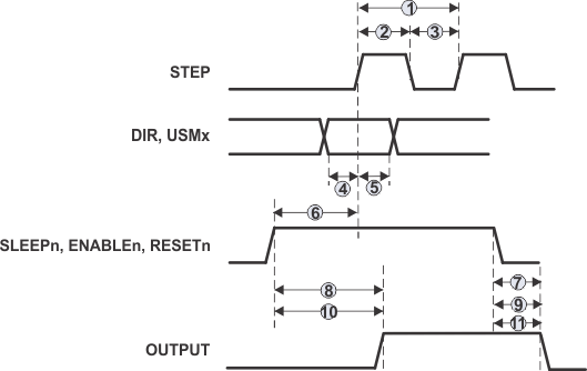 Figure 1. Timing Diagram
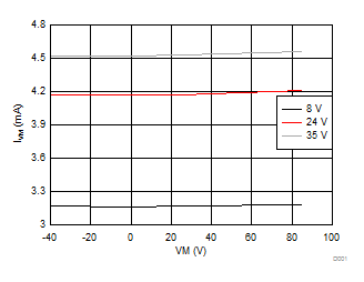
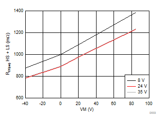
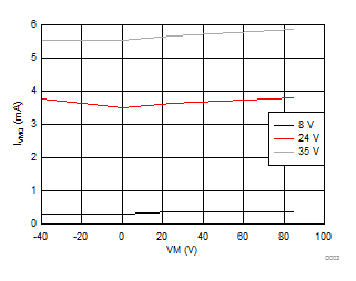
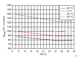
6.8 Typical Characteristics
