SLVS913E January 2009 – January 2016 DRV8823
PRODUCTION DATA.
- 1 Features
- 2 Applications
- 3 Description
- 4 Revision History
- 5 Pin Configuration and Functions
- 6 Specifications
- 7 Detailed Description
- 8 Application and Implementation
- 9 Power Supply Recommendations
- 10Layout
- 11Device and Documentation Support
- 12Mechanical, Packaging, and Orderable Information
6 Specifications
6.1 Absolute Maximum Ratings
over operating free-air temperature (unless otherwise noted)(1) (2)| MIN | MAX | UNIT | |||
|---|---|---|---|---|---|
| VM | Power supply voltage | –0.3 | 34 | V | |
| VI | Logic input voltage(4) | –0.5 | 5.75 | V | |
| IO(peak) | Peak motor drive output current, t < 1 μs | Internally limited | |||
| IO | Motor drive output current(3) | 1.5 | A | ||
| PD | Continuous total power dissipation | See Dissipation Ratings | |||
| TJ | Operating virtual junction temperature | –40 | 150 | °C | |
| TA | Operating ambient temperature | –40 | 85 | °C | |
| Tstg | Storage temperature | –60 | 150 | °C | |
(1) Stresses beyond those listed under Absolute Maximum Ratings may cause permanent damage to the device. These are stress ratings only, and functional operation of the device at these or any other conditions beyond those indicated under Recommended Operating Conditions is not implied. Exposure to absolute–maximum–rated conditions for extended periods may affect device reliability.
(2) All voltage values are with respect to network ground terminal.
(3) Power dissipation and thermal limits must be observed.
(4) Input pins may be driven in this voltage range regardless of presence or absence of VM.
6.2 ESD Ratings
| VALUE | UNIT | |||
|---|---|---|---|---|
| V(ESD) | Electrostatic discharge | Human body model (HBM), per ANSI/ESDA/JEDEC JS-001, all pins(1) | ±2000 | V |
| Charged device model (CDM), per JEDEC specification JESD22-C101, all pins(2) | ±1000 | |||
(1) JEDEC document JEP155 states that 500-V HBM allows safe manufacturing with a standard ESD control process.
(2) JEDEC document JEP157 states that 250-V CDM allows safe manufacturing with a standard ESD control process.
6.3 Recommended Operating Conditions
over operating free-air temperature range (unless otherwise noted)| MIN | NOM | MAX | UNIT | ||
|---|---|---|---|---|---|
| VM | Motor power supply voltage range | 8 | 32 | V | |
| IMOT | Continuous motor drive output current(1) | 1 | 1.5 | A | |
| VREF | VREF input voltage(2) | 1 | 4 | V | |
(1) Power dissipation and thermal limits must be observed.
(2) Operational at VREF between 0 and 1 V, but accuracy is degraded.
6.4 Thermal Information
| THERMAL METRIC(1) | DRV8823 | UNIT | |
|---|---|---|---|
| DCA (HTSSOP) | |||
| 48 PINS | |||
| RθJA | Junction-to-ambient thermal resistance | 31.3 | °C/W |
| RθJC(top) | Junction-to-case (top) thermal resistance | 16.3 | °C/W |
| RθJB | Junction-to-board thermal resistance | 15 | °C/W |
| ψJT | Junction-to-top characterization parameter | 0.6 | °C/W |
| ψJB | Junction-to-board characterization parameter | 14.9 | °C/W |
| RθJC(bot) | Junction-to-case (bottom) thermal resistance | 0.6 | °C/W |
(1) For more information about traditional and new thermal metrics, see the Semiconductor and IC Package Thermal Metrics application report, SPRA953.
6.5 Electrical Characteristics
over operating free-air temperature range (unless otherwise noted)| PARAMETER | TEST CONDITIONS | MIN | TYP | MAX | UNIT | |
|---|---|---|---|---|---|---|
| POWER SUPPLIES | ||||||
| IVM | VM operating supply current | VM = 24 V, no loads | 5 | 8 | mA | |
| VUVLO | VM undervoltage lockout voltage | VM rising | 6.5 | 8 | V | |
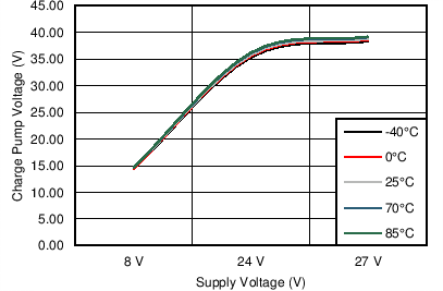
| VCP | Charge pump voltage | Relative to VM | 12 | V | ||
| VV3P3 | VV3P3 output voltage | 3.2 | 3.3 | 3.4 | V | |
| LOGIC-LEVEL INPUTS (INTERNAL PULLDOWNS) | ||||||
| VIL | Input low voltage | 0.7 | V | |||
| VIH | Input high voltage | 2 | V | |||
| VHYS | Input hysteresis | 0.3 | 0.45 | 0.6 | V | |
| IIN | Input current (internal pulldown current) |
VIN = 3.3 V | 100 | μA | ||
| OVERTEMPERATURE PROTECTION | ||||||
| TTSD | Thermal shutdown temperature | Die temperature | 150 | °C | ||
| MOTOR DRIVERS | ||||||
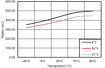
| Rds(on) | Motor 1 FET on resistance (each individual FET) |
VM = 24 V, IO = 0.8 A, TJ = 25°C | 0.25 | Ω | ||
| VM = 24 V, IO = 0.8 A, TJ = 85°C | 0.31 | 0.37 | ||||
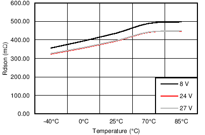
| Rds(on) | Motor 2 FET on resistance (each individual FET) |
VM = 24 V, IO = 0.8 A, TJ = 25°C | 0.3 | Ω | ||
| VM = 24 V, IO = 0.8 A, TJ = 85°C | 0.38 | 0.45 | ||||
| IOFF | Off-state leakage current | ±12 | μA | |||
| fPWM | Motor PWM frequency(1) | 45 | 50 | 55 | kHz | |
| tBLANK | ITRIP blanking time(2) | 3.75 | μs | |||
| tF | Output fall time | 50 | 300 | ns | ||
| tR | Output rise time | 50 | 300 | ns | ||
| IOCP | Overcurrent protect level | 1.5 | 3 | 4.5 | A | |
| tOCP | Overcurrent protect trip time | 2.5 | μs | |||
| tMD | Mixed decay percentage | Measured from beginning of PWM cycle | 75% | |||
| CURRENT CONTROL | ||||||
| IREF | xVREF input current | xVREF = 3.3 V | –3 | 3 | μA | |
| ΔICHOP | Chopping current accuracy | xVREF = 2.5 V, derived from V3P3; 71% to 100% current | –5% | 5% | ||
| xVREF = 2.5 V, derived from V3P3; 20% to 56% current | –10% | 10% | ||||
(1) Factory option 100 kHz.
(2) Factory options for 2.5, 5, or 6.25 μs.
6.6 Timing Requirements
over operating free-air temperature range (unless otherwise noted)| NO. | MIN | MAX | UNIT | ||
|---|---|---|---|---|---|
| 1 | tCYC | Clock cycle time | 62 | ns | |
| 2 | tCLKH | Clock high time | 25 | ns | |
| 3 | tCLKL | Clock low time | 25 | ns | |
| 4 | tSU(SDATA) | Setup time, SDATA to SCLK | 5 | ns | |
| 5 | tH(DATA) | Hold time, SDATA to SCLK | 1 | ns | |
| 6 | tSU(SCS) | Setup time, SCS to SCLK | 5 | ns | |
| 7 | tH(SCS) | Hold time, SCS to SCLK | 1 | ns | |
6.7 Dissipation Ratings
| BOARD | PACKAGE | RθJA | DERATING FACTOR ABOVE TA = 25°C |
TA < 25°C | TA = 70°C | TA = 85°C |
|---|---|---|---|---|---|---|
| Low-K(1) | DCA | 75.7°C/W | 13.2 mW/°C | 1.65 W | 1.06 W | 0.86 W |
| Low-K(2) | 32°C/W | 31.3 mW/°C | 3.91 W | 2.50 W | 2.03 W | |
| High-K(3) | 30.3°C/W | 33 mW/°C | 4.13 W | 2.48 W | 2.15 W | |
| High-K(4) | 22.3°C/W | 44.8 mW/°C | 5.61 W | 3.59 W | 2.91 W |
(1) The JEDEC low-K board used to derive this data was a 76-mm × 114-mm, 2-layer, 1.6-mm thick PCB with no backside copper.
(2) The JEDEC low-K board used to derive this data was a 76-mm × 114-mm, 2-layer, 1.6-mm thick PCB with 25-cm2, 2-oz copper on back side.
(3) The JEDEC high-K board used to derive this data was a 76-mm × 114-mm, 4-layer, 1.6-mm thick PCB with no backside copper and solid 1-oz internal ground plane.
(4) The JEDEC high-K board used to derive this data was a 76-mm × 114-mm, 4-layer, 1.6-mm thick PCB with 25-cm2, 1-oz copper on backside and solid 1-oz internal ground plane.
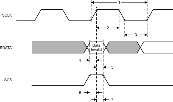 Figure 1. Timing Diagram
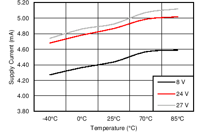
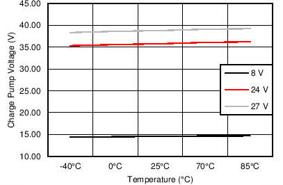
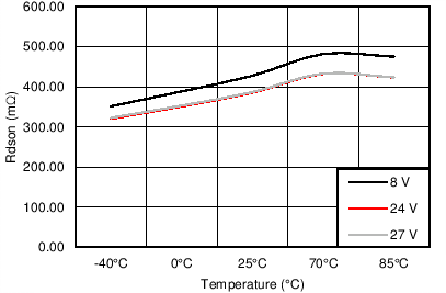
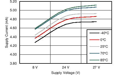
6.8 Typical Characteristics
