SLVSB19D February 2012 – March 2015 DRV8834
PRODUCTION DATA.
- 1 Features
- 2 Applications
- 3 Description
- 4 Simplified Schematic
- 5 Revision History
- 6 Pin Configuration and Functions
- 7 Specifications
- 8 Detailed Description
- 9 Application and Implementation
- 10Power Supply Recommendations
- 11Layout
- 12Device and Documentation Support
- 13Mechanical, Packaging, and Orderable Information
パッケージ・オプション
メカニカル・データ(パッケージ|ピン)
サーマルパッド・メカニカル・データ
発注情報
7 Specifications
7.1 Absolute Maximum Ratings
over operating free-air temperature range (unless otherwise noted)(1)(2)| MIN | MAX | UNIT | |||
|---|---|---|---|---|---|
| VM | Power supply voltage | –0.3 | 11.8 | V | |
| AVREF, BVREF, VINT, ADECAY, BDECAY |
Analog input pin voltage | –0.5 | 3.6 | V | |
| Digital input pin voltage | –0.5 | 7 | V | ||
| xISEN pin voltage | –0.3 | 0.5 | V | ||
| Peak motor drive output current, t < 1 µs | Internally limited | A | |||
| TJ | Operating virtual junction temperature | –40 | 150 | °C | |
| Tstg | Storage temperature | –60 | 150 | °C | |
(1) Stresses beyond those listed under absolute maximum ratings may cause permanent damage to the device. These are stress ratings only, and functional operation of the device at these or any other conditions beyond those indicated under recommended operating conditions is not implied. Exposure to absolute–maximum–rated conditions for extended periods may affect device reliability.
(2) All voltage values are with respect to network ground terminal.
7.2 ESD Ratings
| VALUE | UNIT | ||||
|---|---|---|---|---|---|
| V(ESD) | Electrostatic discharge | Human body model (HBM), per ANSI/ESDA/JEDEC JS-001, all pins(1) | ±4000 | V | |
| Charged device model (CDM), per JEDEC specification JESD22-C101, all pins(2) | ±1500 | ||||
(1) JEDEC document JEP155 states that 500-V HBM allows safe manufacturing with a standard ESD control process.
(2) JEDEC document JEP157 states that 250-V CDM allows safe manufacturing with a standard ESD control process.
7.3 Recommended Operating Conditions
TA = 25°C, over operating free-air temperature range (unless otherwise noted)| MIN | NOM | MAX | UNIT | ||
|---|---|---|---|---|---|
| VM | Motor power supply voltage range(1) | 2.5 | 10.8 | V | |
| VREF | VREF input voltage range(2) | 1 | 2.1 | V | |
| IVINT | VINT external load current | 1 | mA | ||
| IVREF | VREF external load current | 400 | µA | ||
| VDIGIN | Digital input pin voltage range | –0.3 | 5.75 | V | |
| IOUT | Continuous RMS or DC output current per bridge(3) | 1.5 | A | ||
(1) RDS(ON) increases and maximum output current is reduced at VM supply voltages below 5 V.
(2) Operational at VREF between 0 V and 1 V, but accuracy is degraded.
(3) Power dissipation and thermal limits must be observed.
7.4 Thermal Information
| THERMAL METRIC(1) | DRV8834 | UNIT | ||
|---|---|---|---|---|
| PWP [HTSSOP] | RGE [VQFN] | |||
| 24 PINS | 24 PINS | |||
| RθJA | Junction-to-ambient thermal resistance | 40.2 | 35.1 | °C/W |
| RθJC(top) | Junction-to-case (top) thermal resistance | 23.7 | 36.6 | |
| RθJB | Junction-to-board thermal resistance | 21.9 | 12.2 | |
| ψJT | Junction-to-top characterization parameter | 0.7 | 0.6 | |
| ψJB | Junction-to-board characterization parameter | 21.7 | 12.2 | |
| RθJC(bot) | Junction-to-case (bottom) thermal resistance | 3.9 | 4 | |
(1) For more information about traditional and new thermal metrics, see the IC Package Thermal Metrics application report, SPRA953.
7.5 Electrical Characteristics
TA = 25°C, over operating free-air temperature range (unless otherwise noted)| PARAMETER | TEST CONDITIONS | MIN | TYP | MAX | UNIT | |
|---|---|---|---|---|---|---|
| POWER SUPPLY | ||||||
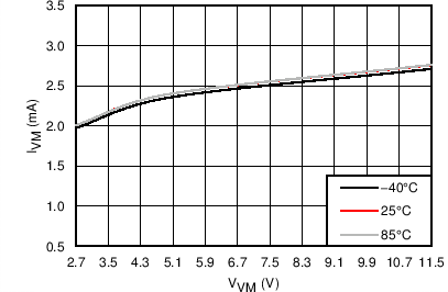
| IVM | VM operating supply current | VM = 5 V, excluding winding current | 2.4 | 4 | mA | |
| VM = 10 V, excluding winding current | 2.75 | |||||
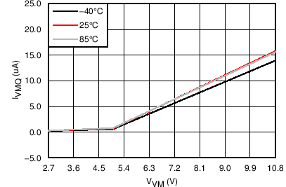
| IVMQ | VM sleep mode supply current | VM = 5 V | 0.6 | 2 | μA | |
| VM = 10 V | 9.6 | |||||
| VUVLO | VM undervoltage lockout voltage | VM falling | 2.39 | V | ||
| INTERNAL REGULATORS | ||||||
| VINT | VINT voltage | VM > 3.3 V, IOUT = 0 A to 1 mA | 2.85 | 3 | 3.15 | V |
| VREFO | VREF voltage | IOUT = 0 A to 400 µA | 1.9 | 2 | 2.1 | V |
| LOGIC-LEVEL INPUTS | ||||||
| VIL | Input low voltage | nSLEEP | 0.5 | V | ||
| All other digital input pins | 0.7 | |||||
| VIH | Input high voltage | nSLEEP | 2.5 | V | ||
| All other digital input pins | 2 | |||||
| VHYS | Input hysteresis | nSLEEP | 0.2 | V | ||
| All except nSLEEP | 0.4 | |||||
| RPD | Input pulldown resistance | nSLEEP | 500 | kΩ | ||
| All except nSLEEP, M0 | 200 | |||||
| IIL | Input low current | VIN = 0 | 1 | μA | ||
| IIN | Input current (M0) | -20 | 20 | µA | ||
| IIH | Input high current | VIN = 3.3 V, nSLEEP | 6.6 | 13 | μA | |
| VIN = 3.3 V, all except nSLEEP | 16.5 | 33 | ||||
| tDEG | Input deglitch time | 312 | 468 | ns | ||
| nFAULT OUTPUT (OPEN-DRAIN OUTPUT) | ||||||
| VOL | Output low voltage | IO = 5 mA | 0.5 | V | ||
| IOH | Output high leakage current | VO = 3.3 V | 1 | μA | ||
| H-BRIDGE FETs | ||||||
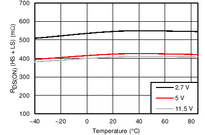
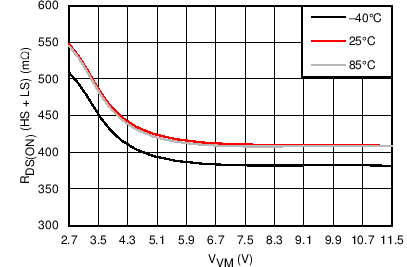
| RDS(ON) | HS FET ON-resistance | VM = 5 V, IO = 500 mA, TJ = 25°C | 160 | 250 | mΩ | |
| VM = 5 V, IO = 500 mA, TJ = 85°C | 190 | |||||
| VM = 2.7 V, IO = 500 mA, TJ = 25°C | 200 | 295 | ||||
| VM = 2.7 V, IO = 500 mA, TJ = 85°C | 240 | |||||
| LS FET ON-resistance | VM = 5 V, IO = 500 mA, TJ = 25°C | 145 | 240 | |||
| VM = 5 V, IO = 500 mA, TJ = 85°C | 180 | |||||
| VM = 2.7 V, IO = 500 mA, TJ = 25°C | 190 | 285 | ||||
| VM = 2.7 V, IO = 500 mA, TJ = 85°C | 235 | |||||
| IOFF | Off-state leakage current | –2 | 2 | μA | ||
| MOTOR DRIVER | ||||||
| fPWM | Current control PWM frequency | Internal PWM frequency | 42.5 | kHz | ||
| tBLANK | Current sense blanking time | VREF > 375 mV or DAC codes > 29% | 2.4 | µs | ||
| VREF < 375 mV or DAC codes < 29% | 1.6 | |||||
| tR | Rise time | VM = 5 V, 16 Ω to GND, 10% to 90% VM | 120 | ns | ||
| tF | Fall time | VM = 5 V, 16 Ω to GND, 10% to 90% VM | 100 | ns | ||
| PROTECTION CIRCUITS | ||||||
| IOCP | Overcurrent protection trip level | 2 | A | |||
| tOCP | Overcurrent protection period | VREF > 375 mV or DAC codes > 29% | 1.6 | µs | ||
| VREF < 375 mV or DAC codes < 29% | 1.1 | |||||
| tTSD | Thermal shutdown temperature | Die temperature | 150 | 160 | 180 | °C |
| CURRENT CONTROL | ||||||
| IREF | VREF input current | VREF = 3.3 V | –1 | 1 | µA | |
| VTRIP | xISEN trip voltage | For 100% current step | xVREF/5 | V | ||
| AISENSE | Current sense amplifier gain | Reference only | 5 | V/V | ||
7.6 Timing Requirements
TA = 25°C, over operating free-air temperature range (unless otherwise noted)| NO. | PARAMETER | CONDITIONS | MIN | TYP | MAX | UNIT |
|---|---|---|---|---|---|---|
| 1 | fSTEP | Step frequency | 250 | kHz | ||
| 2 | tWH(STEP) | Pulse duration, STEP high | 1.9 | µs | ||
| 3 | tWL(STEP) | Pulse duration, STEP low | 1.9 | µs | ||
| 4 | tSU(STEP) | Setup time, command to STEP rising | 200 | ns | ||
| 5 | tH(STEP) | Hold time, command to STEP rising | 1 | µs | ||
| 6 | tWAKE | Wake-up time, nSLEEP inactive to STEP | 1 | ms |
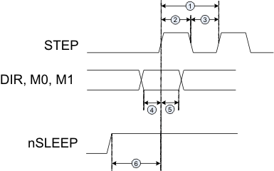 Figure 1. Timing Diagram
7.7 Typical Characteristics
