SNLS430C October 2012 – August 2014 DS125BR111
PRODUCTION DATA.
- 1 Features
- 2 Applications
- 3 Description
- 4 Simplified Schematic
- 5 Revision History
- 6 Pin Configuration and Functions
- 7 Specifications
- 8 Detailed Description
- 9 Application and Implementation
- 10Power Supply Recommendations
- 11Layout
- 12Device and Documentation Support
- 13Mechanical, Packaging, and Orderable Information
パッケージ・オプション
メカニカル・データ(パッケージ|ピン)
- RTW|24
サーマルパッド・メカニカル・データ
- RTW|24
発注情報
7 Specifications
7.1 Absolute Maximum Ratings
over operating free-air temperature range (unless otherwise noted) (1)| MIN | MAX | UNIT | ||
|---|---|---|---|---|
| Supply Voltage (VDD - 2.5 V) | -0.5 | +2.75 | V | |
| Supply Voltage (VIN - 3.3 V) | -0.5 | +4.0 | V | |
| LVCMOS Input/Output Voltage | -0.5 | +4.0 | V | |
| CML Input Voltage | -0.5 | VDD + 0.5 | V | |
| CML Input Current | -30 | +30 | mA | |
(1) Stresses beyond those listed under Absolute Maximum Ratings may cause permanent damage to the device. These are stress ratings only, which do not imply functional operation of the device at these or any other conditions beyond those indicated under Recommended Operating Conditions. Exposure to absolute-maximum-rated conditions for extended periods may affect device reliability.
7.2 Handling Ratings
| MIN | MAX | UNIT | |||
|---|---|---|---|---|---|
| Tstg | Storage temperature range | -40 | 125 | °C | |
| Tsolder | Lead Temperature Range Soldering (4 sec.)(1) | 260 | °C | ||
| V(ESD) | Electrostatic discharge | Human body model (HBM), per ANSI/ESDA/JEDEC JS-001, all pins(2) | -5000 | 5000 | V |
| Charged device model (CDM), per JEDEC specification JESD22-C101, all pins(3) | -1250 | 1250 | |||
(1) For soldering specifications: See application note SNOA549.
(2) JEDEC document JEP155 states that 500 V HBM allows safe manufacturing with a standard ESD control process.
(3) JEDEC document JEP157 states that 250 V CDM allows safe manufacturing with a standard ESD control process.
7.3 Recommended Operating Conditions
over operating free-air temperature range (unless otherwise noted)| MIN | NOM | MAX | UNIT | |
|---|---|---|---|---|
| Supply Voltage (2.5 V mode) | 2.375 | 2.5 | 2.625 | V |
| Supply Voltage (3.3 V mode) | 3.0 | 3.3 | 3.6 | V |
| Ambient Temperature | -40 | 25 | +85 | °C |
| SMBus (SDA, SCL) | 3.6 | V | ||
| Supply Noise up to 50 MHz(2) | 100 | mVp-p |
7.4 Thermal Information
| THERMAL METRIC(1) | DS125BR111 | UNIT | |
|---|---|---|---|
| RTW | |||
| 24 PINS | |||
| RθJA | Junction-to-ambient thermal resistance | 35.0 | °C/W |
| RθJC(top) | Junction-to-case (top) thermal resistance | 34.0 | |
| RθJB | Junction-to-board thermal resistance | 13.4 | |
| ψJT | Junction-to-top characterization parameter | 0.3 | |
| ψJB | Junction-to-board characterization parameter | 13.4 | |
| RθJC(bot) | Junction-to-case (bottom) thermal resistance | 3.3 | |
(1) For more information about traditional and new thermal metrics, see the IC Package Thermal Metrics application report, SPRA953.
7.5 Electrical Characteristics
over operating free-air temperature range (unless otherwise noted)| PARAMETER | TEST CONDITIONS | MIN | TYP | MAX | UNIT | |
|---|---|---|---|---|---|---|
| POWER | ||||||
| IDD | Current Consumption | VODx_DB = 0, EQ = 0, VOD_SEL = 1, RXDET = 1, PWDN = 0 VIN = 2.625 or 3.6 V |
40 | 60 | mA | |
| Power Down Current Consumption | PWDN = 1 | 7 | 13 | mA | ||
| VDD | Integrated LDO Regulator | VIN = 3.0 - 3.6 V | 2.375 | 2.5 | 2.625 | V |
| LVCMOS / LVTTL DC SPECIFICATIONS | ||||||
| Vih25 | High Level Input Voltage | 2.5 V Supply Mode | 1.7 | VDD | V | |
| Vih33 | High Level Input Voltage | 3.3 V Supply Mode | 1.7 | VIN | V | |
| Vil | Low Level Input Voltage | 0 | 0.7 | V | ||
| Voh | High Level Output Voltage (DONE pin) |
Ioh = −4 mA | 2.0 | V | ||
| Vol | Low Level Output Voltage (DONE pin) |
Iol = 4 mA | 0.4 | V | ||
| Iih | Input High Current (PWDN pin) | VIN = 3.6 V, LVCMOS = 3.6 V |
-15 | +15 | µA | |
| Iil | Input Low Current (PWDN pin) | VIN = 3.6 V, LVCMOS = 0 V |
-15 | +15 | µA | |
| 4-LEVEL INPUT DC SPECIFICATIONS | ||||||
| Iih | Input High Current with internal resistors (4–level input pin) |
VIN = 3.6 V, LVCMOS = 3.6 V |
+20 | +80 | µA | |
| Iil | Input Low Current with internal resistors (4–level input pin) |
VIN = 3.6 V, LVCMOS = 0 V |
-160 | -40 | µA | |
| Vth | Threshold 0 / R | VDD = 2.5 V (2.5 V supply mode) Internal LDO Disabled See Table 1 for details |
0.40 | V | ||
| Threshold R / Float | 1.25 | |||||
| Threshold Float / 1 | 2.1 | |||||
| Threshold 0 / R | VIN = 3.3 V (3.3 V supply mode) Internal LDO Enabled See Table 1 for details. |
0.55 | V | |||
| Threshold R / Float | 1.65 | |||||
| Threshold Float / 1 | 2.7 | |||||
| CML RECEIVER INPUTS (IN_n+, IN_n-) | ||||||
| RLRX-diff | RX Differential return loss | SDD11 10 MHz | -19 | dB | ||
| SDD11 2 GHz | -14 | |||||
| SDD11 6-11.1 GHz | -8 | |||||
| RLRX-cm | RX Common mode return loss | 0.05 - 5 GHz | -10 | dB | ||
| ZRX-dc | RX DC common mode impedance | Tested at VDD = 2.5 V | 40 | 50 | 60 | Ω |
| ZRX-diff-dc | RX DC differential mode impedance | Tested at VDD = 2.5 V | 80 | 100 | 120 | Ω |
| VRX-signal-det-diff-pp | Signal detect assert level | SD_TH = F (float), 0101 pattern at 12 Gbps |
50 | mVp-p | ||
| VRX-idle-det-diff-pp | Signal detect de-assert level | SD_TH = F (float), 0101 pattern at 12 Gbps |
37 | mVp-p | ||
| HIGH SPEED OUTPUTS | ||||||
| TTX-RISE-FALL | Transmitter rise/fall time (3) | 20% to 80% of differential output voltage | 40 | ps | ||
| TRF-MISMATCH | Transmitter rise/fall mismatch (4) | 20% to 80% of differential output voltage | 0.01 | UI | ||
| RLTX-DIFF | TX Differential return loss | SDD22 10 MHz - 2 GHz | -15 | dB | ||
| SDD22 5.5 GHz | -12 | |||||
| SDD22 11.1 GHz | -10 | dB | ||||
| RLTX-CM | TX Common mode return loss | 0.05 - 5 GHz | -10 | dB | ||
| ZTX-DIFF-DC | DC differential TX impedance | 100 | Ω | |||
| ITX-SHORT | Transmitter short circuit current limit | Total current, output shorted to VDD or GND | 20 | mA | ||
| VTX-CM-DC-ACTIVE-IDLE-DELTA | Absolute delta of DC common mode voltage during L0 and electrical idle | 100 | mV | |||
| VTX-CM-DC-LINE-DELTA | Absolute delta of DC common mode voltage between TX+ and TX- | 25 | mV | |||
| HIGH SPEED OUTPUTS | ||||||
| VTX-diff1-pp | Output Voltage Differential Swing | Differential measurement with OUTx+ and OUTx-, AC-Coupled and terminated by 50 Ω to GND, Inputs AC-Coupled, VODx_DB = 0 dB, VID = 600 mVp-p VOD = 001'b (0.7*VID) |
440 | 500 | 550 | mVp-p |
| VTX-diff2-pp | Output Voltage Differential Swing | Differential measurement with OUTx+ and OUTx-, AC-Coupled and terminated by 50 Ω to GND, Inputs AC-Coupled, VODx_DB = 0 dB, VID = 1000 mVp-p VOD = 001'b (0.7*VID) (5) |
630 | 700 | 740 | mVp-p |
| VTX-diff3-pp | Output Voltage Differential Swing | Differential measurement with OUTx+ and OUTx-, AC-Coupled and terminated by 50 Ω to GND, Inputs AC-Coupled, VODx_DB = 0 dB, VID = 600 mVp-p VOD = 111'b (1.05*VID) (5) |
570 | 650 | 740 | mVp-p |
| VTX-diff4-pp | Output Voltage Differential Swing | Differential measurement with OUTx+ and OUTx-, AC-Coupled and terminated by 50 Ω to GND, Inputs AC-Coupled, VODx_DB = 0 dB, VID = 1000 mVp-p VOD = 111'b (1.05*VID) (5) |
800 | 1010 | 1215 | mVp-p |
| TTX-IDLE-DATA | Time to transition to valid differential signal after idle | VID = 1.0 Vp-p, 3 Gbps | 0.04 | ns | ||
| TTX-DATA-IDLE | Time to transition to idle after differential signal | VID = 1.0 Vp-p, 3 Gbps | 0.70 | ns | ||
| TPD | Differential Propagation Delay | EQ = Level 1 to Level 4 | 70 | ps | ||
| EQUALIZATION | ||||||
| DJE1 | Residual Deterministic Jitter at 6 Gbps | Input: 5” Differential Stripline, 5mil trace width, FR4, VID = 0.8 Vp-p, PRBS15, EQ = 0x01, VOD = 111'b, VODx_DB = 0 dB |
0.06 | UI | ||
| DJE2 | Residual Deterministic Jitter at 12 Gbps | Input: 5” Differential Stripline, 5mil trace width, FR4, VID = 0.8 Vp-p, PRBS15, EQ = 0x01, VOD = 111'b, VODx_DB = 0 dB |
0.12 | UI | ||
| RJADD1 | Additive Random Jitter (1) | Evaluation Module (EVM) only, FR4, VID = 0.8 Vp-p, PRBS7, EQ = 0x00, VOD = 111'b, VODx_DB = 0 dB |
< 300 | fs RMS | ||
| RJADD2 | Additive Random Jitter (1) | Input: 10" Differential Stripline, 5 mil trace width, FR4, VID = 0.8 Vp-p, PRBS7, EQ = 0x03, VOD = 111'b, VODx_DB = 0 dB |
< 400 | fs RMS | ||
(1) Additive random jitter is given in RMS value by the following equation: RJADD = √[(Output Jitter)2 - (Input Jitter)2] . The typical source input jitter for these measurements is 150 fs RMS.
(2) Allowed supply noise (mVp-p sine wave) under typical conditions.
(3) Rise / Fall time measurements will vary based on EQ setting, Input Amplitude, and input edge rate.
(4) Mismatch between rise time and fall time for a given channel.
(5) The output VOD level is not fixed. It will be adjusted automatically based on the VID input amplitude level and the frequency content. The DS125BR111 repeater is designed to be transparent, so the TX-FIR (de-emphasis) is passed to the RX to support handshake negotiation link training.
7.6 Electrical Characteristics — Serial Management Bus Interface
Over recommended operating supply and temperature ranges unless other specified.| PARAMETER | TEST CONDITIONS | MIN | TYP | MAX | UNIT | |
|---|---|---|---|---|---|---|
| SERIAL BUS INTERFACE DC SPECIFICATIONS | ||||||
| VIL | Data, Clock Input Low Voltage | 0.8 | V | |||
| VIH | Data, Clock Input High Voltage | 2.1 | 3.6 | V | ||
| VOL | Output Low Voltage | SDA or SCL, IOL = 1.25 mA | 0 | 0.36 | V | |
| VDD | Nominal Bus Voltage | 2.375 | 3.6 | V | ||
| IIH-pin | Input Leakage Per Device pin | +20 | +150 | µA | ||
| IIL-pin | Input Leakage Per Device pin | -160 | -40 | µA | ||
| CI | Capacitance for SDA and SCL | See(1)(2) | < 5 | pF | ||
| RTERM | External Termination Resistance pull to VDD = 2.5 V ± 5% OR 3.3 V ± 10% | Pullup VDD = 3.3 V(1)(2)(3) | 2000 | Ω | ||
| Pullup VDD = 2.5 V(1)(2)(3) | 1000 | Ω | ||||
(1) Typical value.
(2) Recommended maximum capacitance load per bus segment is 400 pF.
(3) Maximum termination voltage should be identical to the device supply voltage.
7.7 Timing Requirements
| PARAMETER | TEST CONDITIONS | MIN | TYP | MAX | UNIT | |
|---|---|---|---|---|---|---|
| SERIAL BUS INTERFACE TIMING SPECIFICATIONS | ||||||
| FSMB | Bus Operating Frequency | ENSMB = VDD (Slave Mode) | 400 | kHz | ||
| ENSMB = FLOAT (Master Mode) (1) | 280 | 400 | 520 | kHz | ||
| tFALL | SCL or SDA Fall Time | Read operation RPU = 4.7 kΩ, Cb < 50 pF |
60 | ns | ||
| tRISE | SCL or SDA Rise Time | Read operation RPU = 4.7 kΩ, Cb < 50 pF |
140 | ns | ||
| tF | Clock/Data Fall Time | See(2) | 300 | ns | ||
| tR | Clock/Data Rise Time | See(2) | 1000 | ns | ||
(1) The external EEPROM device address byte must be 0xA0 and capable of 1 MHz operation at 2.5 V and 3.3 V.
(2) Compliant to SMBus 2.0 physical layer specification. See System Management Bus (SMBus) Specification Version 2.0, section 3.1.1 SMBus common AC specifications for details.
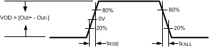 Figure 1. Output Rise And Fall Transition Time
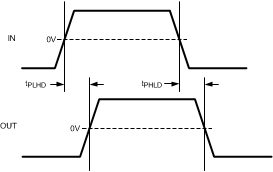 Figure 2. Propagation Delay Timing Diagram
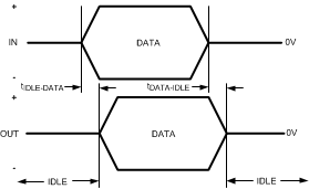 Figure 3. Transmit Idle-Data and Data-Idle Response Time
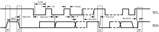 Figure 4. SMBus Timing Parameters
7.8 Typical Characteristics
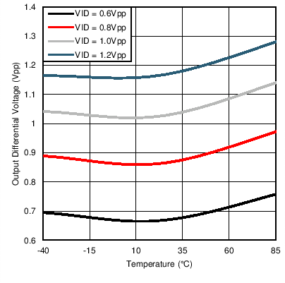
| Test Conditions | ||
| Data Rate/Test Pattern: | 1.5625 Gbps / 101010 Repeating Pattern |
|
| VOD: | Level 6 | |
| EQ: | Level 1 | |
| VOD_DB: | 000'b | |
| VDD: | 2.5 V | |
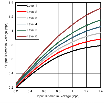
| Test Conditions | ||
| Data Rate/Test Pattern: | 1.5625 Gbps / 101010 Repeating Pattern | |
| EQ: | Minimum | |
| VOD_DB: | 000'b | |
| Temperature: | 25°C | |
| VDD: | 2.5 V | |
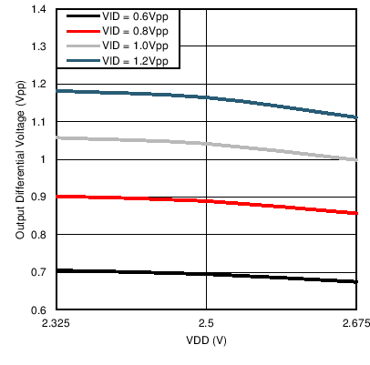
| Test Conditions | ||
| Data Rate/Test Pattern: | 1.5625 Gbps / 101010 Repeating Pattern |
|
| VOD: | Level 6 | |
| EQ: | Level 1 | |
| VOD_DB: | 000'b | |
| Temperature: | 25°C | |