JAJS617C July 1999 – July 2016 DS90LV048A
PRODUCTION DATA.
- 1 特長
- 2 アプリケーション
- 3 概要
- 4 改訂履歴
- 5 Pin Configuration and Functions
- 6 Specifications
- 7 Parameter Measurement Information
- 8 Detailed Description
- 9 Application and Implementation
- 10Power Supply Recommendations
- 11Layout
- 12デバイスおよびドキュメントのサポート
- 13メカニカル、パッケージ、および注文情報
パッケージ・オプション
メカニカル・データ(パッケージ|ピン)
サーマルパッド・メカニカル・データ
発注情報
7 Parameter Measurement Information
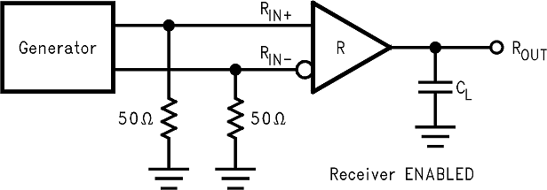
 Figure 15. Receiver Propagation Delay and Transition Time Test Circuit
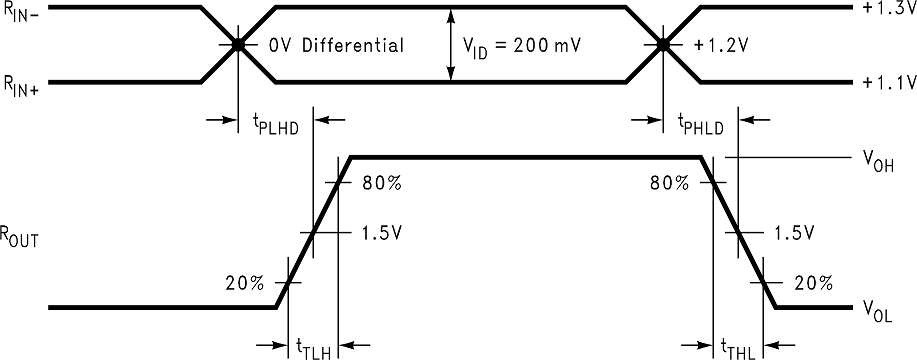
 Figure 16. Receiver Propagation Delay and Transition Time Waveforms

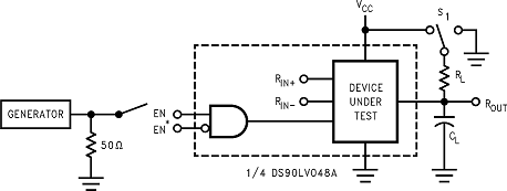
CL includes load and test jig capacitance.
S1 = VCC for tPZL and tPLZ measurements.
S1 = GND for tPZH and tPHZ measurements.
Figure 17. Receiver TRI-STATE Delay Test Circuit
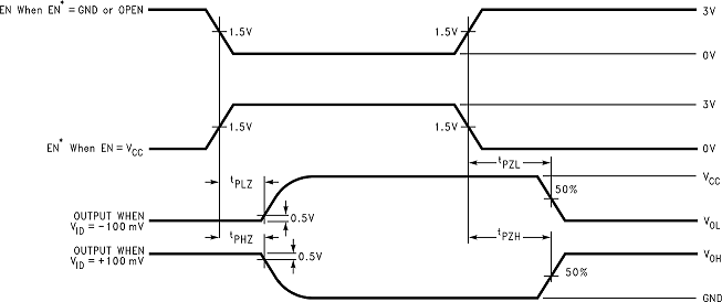
S1 = VCC for tPZL and tPLZ measurements.
S1 = GND for tPZH and tPHZ measurements.
 Figure 18. Receiver TRI-STATE Delay Waveforms