JAJSCV7E august 2016 – november 2020 DS90UB933-Q1
PRODUCTION DATA
- 1
- 1 特長
- 2 アプリケーション
- 3 概要
- 4 Revision History
- 5 Pin Configuration and Functions
-
6 Specifications
- 6.1 Absolute Maximum Ratings
- 6.2 ESD Ratings
- 6.3 Recommended Operating Conditions
- 6.4 Thermal Information
- 6.5 Electrical Characteristics
- 6.6 Recommended Serializer Timing For PCLK
- 6.7 AC Timing Specifications (SCL, SDA) - I2C-Compatible
- 6.8 Bidirectional Control Bus DC Timing Specifications (SCL, SDA) - I2C-Compatible
- 6.9 Serializer Switching Characteristics
- 6.10 Timing Diagrams
- 6.11 Typical Characteristics
- 7 Detailed Description
- 8 Application and Implementation
- 9 Power Supply Recommendations
- 10Layout
- 11Device and Documentation Support
パッケージ・オプション
メカニカル・データ(パッケージ|ピン)
- RTV|32
サーマルパッド・メカニカル・データ
- RTV|32
発注情報
7.4.1 DS90UB933/934 Operation With External Oscillator as Reference Clock
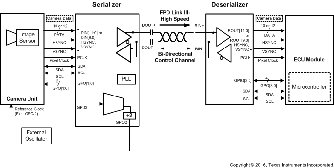
In some applications, the pixel clock that comes from the imager can have jitter which exceeds the tolerance of the DS90UB933/934/964 chipsets. In this case, operate the DS90UB933-Q1 device by using an external clock source as the reference clock for the DS90UB933/934/964 chipsets. This is the recommended operating mode. The external oscillator clock output goes through a divide-by-2 circuit in the DS90UB933-Q1 serializer, and this divided clock output is used as the reference clock for the imager. The output data and pixel clock from the imager are then fed into the DS90UB933-Q1 device. Figure 7-4 shows the operation of the DS90UB33/934 chipsets while using an external automotive grade oscillator.
 Figure 7-4 DS90UB933-Q1/934-Q1 Operation in the External Oscillator Mode
When the DS90UB933-Q1 device is operated using an external oscillator, the GPO3 pin on the DS90UB933-Q1 is the input pin for the external oscillator. In applications where the DS90UB933-Q1 device is operated from an external oscillator, the divide-by-2 circuit in the DS90UB933-Q1 device feeds back the divided clock output to the imager device through GPO2 pin. The pixel clock to external oscillator ratios must be fixed for the 12–bit mode and the 10–bit mode. In the 10-bit mode, the pixel clock frequency divided by the external oscillator frequency must be 2. In the 12-bit mode, the pixel clock frequency divided by the external oscillator frequency must be 1.5. For example, if the external oscillator frequency is 48 MHz in the 10-bit mode, the pixel clock frequency of the imager must be twice of the external oscillator frequency, that is, 96 MHz. If the external oscillator frequency is 48 MHz in the 12-bit mode, the pixel clock frequency of the imager must be 1.5 times of the external oscillator frequency, that is, 72 MHz. For the range of PCLK frequency and the external clock input frequency to GPO3 in 10-bit and 12-bit modes, see Section 6.3.
When PCLK signal edge is detected, and 0x03[1] = 0, the DS90UB933-Q1 switches from internal oscillator mode to an external PCLK. Upon removal of PCLK input, the device switches back into internal oscillator mode. In external oscillator mode, GPO2 and GPO3 on the serializer cannot act as the output of the input signal coming from GPIO2 or GPIO3 on the deserializer.
| MODE | GPIO3 XCLKIN | GPIO2 XCLKOUT = XCLKIN / 2 | RATIO | INPUT PCLK FREQUENCY = XLCKIN * RATIO |
|---|---|---|---|---|
| 10-bit | 48 MHz | 24 MHz | 2 | 96 MHz |
| 12-bit | 48 MHz | 24 MHz | 1.5 | 72 MHz |