SLLSEM6B April 2015 – August 2015 HD3SS2522
PRODUCTION DATA.
- 1 Features
- 2 Applications
- 3 Description
- 4 Revision History
- 5 Pin Configuration and Functions
- 6 Specifications
- 7 Detailed Description
- 8 Application and Implementation
- 9 Power Supply Recommendations
- 10Layout
- 11Device and Documentation Support
- 12Mechanical, Packaging, and Orderable Information
8 Application and Implementation
NOTE
Information in the following applications sections is not part of the TI component specification, and TI does not warrant its accuracy or completeness. TI’s customers are responsible for determining suitability of components for their purposes. Customers should validate and test their design implementation to confirm system functionality.
8.1 Application Information
The HD3SS2522 is a high speed switch with integrated DFP CC controller. The HD3SS2522 can be implemented in any USB Type-C DFP applications in conjunction with VBUS and VCONN switches.
8.2 USB Type-C DFP Typical Application
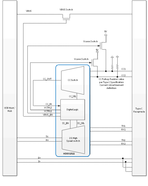
This section depicts the typical Type-C system with a USB Host or Hub. The Type C receptacle in this system is a DFP only providing VBUS and VCONN upon the connection of UFP device. The HD3SS2522 DFP CC controller determines the UFP attachment and provides VBUS and VCONN based upon the Type-C specification state diagram and timing definition.

8.2.1 Design Requirements
For this design example, use the parameters shown in Table 1.
Table 1. Design Parameters
| PARAMETER | VALUE |
|---|---|
| VCC | 3.3 V |
| AxP/N, BxP/N, CxP/N VCM Voltage | 0 V – 2 V |
| CC_IN, CC_OUT, CC1, CC2 | 0 V –3.3 V |
| Control Pin Vmax for Low | 0.8 V |
| Control Pin Vmax for High | 2 V |
8.2.2 Detailed Design Procedure
8.2.2.1 USB Type-C Current Advertising
HD3SS2522 can be used to advertise USB Type-C current in conjunction with pull up resistors to CC1 and CC2 pins. These pull up resistors must meet the Type C spec requirements. The IMODE1 and IMODE2 setting must match the CC resistor configuration for the current mode: default, mid or high.
8.2.2.2 VCONN and VBUS Power Switch Control
VCTRL1# and VCTRL2# are outputs from the HD3SS2522 CC controller to enable or disable the VCONN switch based upon the orientation detection, audio accessory termination Ra detection, and/or fault condition.
VBUS_EN is an output from the HD3SS2522 CC controller to enable VBUS switch. Upon detection of UFP attachment, the VBUS_EN is asserted to enable VBUS switch.
8.2.2.3 Firmware Upgradability
If necessary, the CC controller firmware (FW) can be updated via GPIO1, GPIO2 and SYS_COM_REQ. Contact Texas Instruments for further assistance with upgrading the FW.
8.2.3 USB Type-C DFP Circuit Schematics with a Type C Receptacle
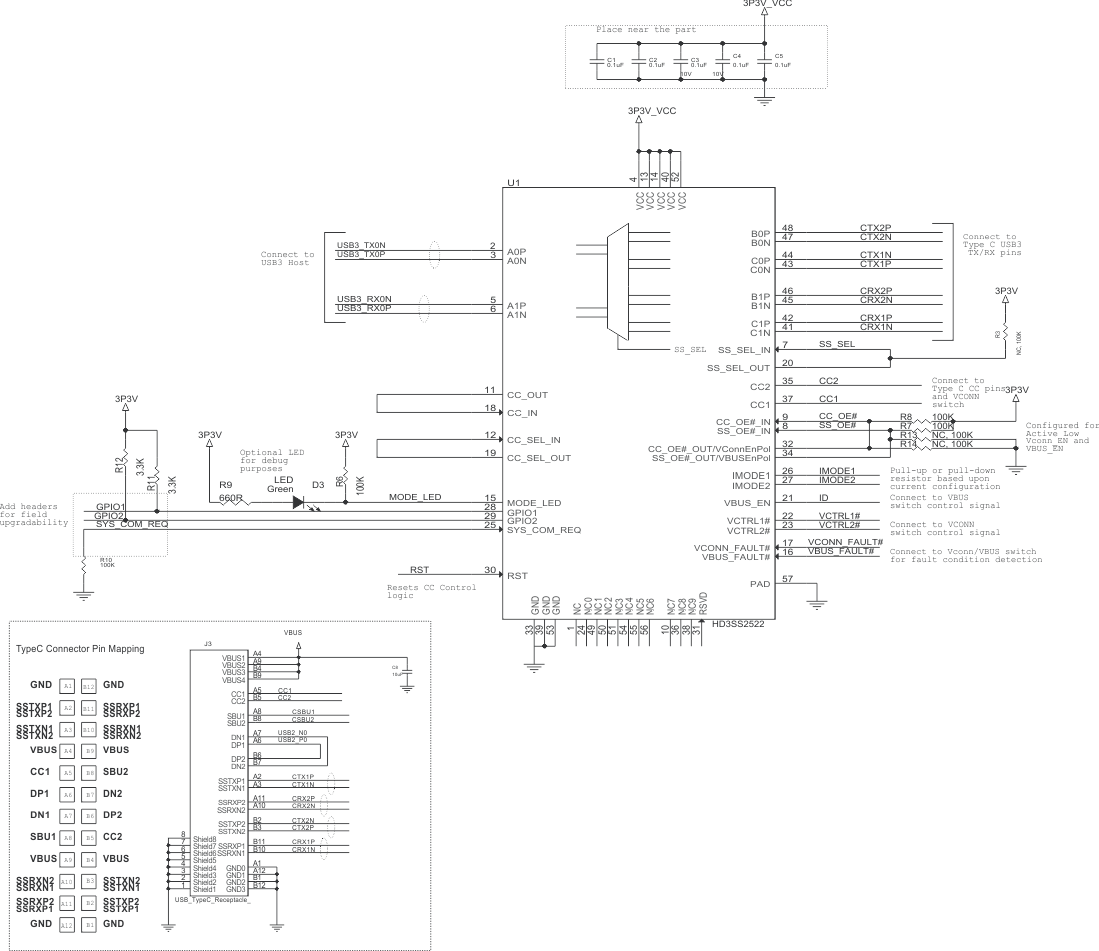
The schematics below depicts the circuit level implementation of the Type C system with HD3SS2522 and a DFP only Type C connector. The system should select a power switch that complies with the Type C specification and application requirements. The power switch can be controlled by the HD3SS2522. See the Detailed Design Procedure section of the datasheet for design details.
 Figure 4. Example Schematics With a Type-C Receptacle