JAJSSC8A November 1996 – February 2024 INA132
PRODUCTION DATA
- 1
- 1特長
- 2アプリケーション
- 3概要
- 4Pin Configuration and Functions
- 5Specifications
- 6Application and Implementation
- 7Device and Documentation Support
- 8Revision History
- 9Mechanical, Packaging, and Orderable Information
パッケージ・オプション
デバイスごとのパッケージ図は、PDF版データシートをご参照ください。
メカニカル・データ(パッケージ|ピン)
- D|8
サーマルパッド・メカニカル・データ
発注情報
6.1.2 Offset Voltage Trim
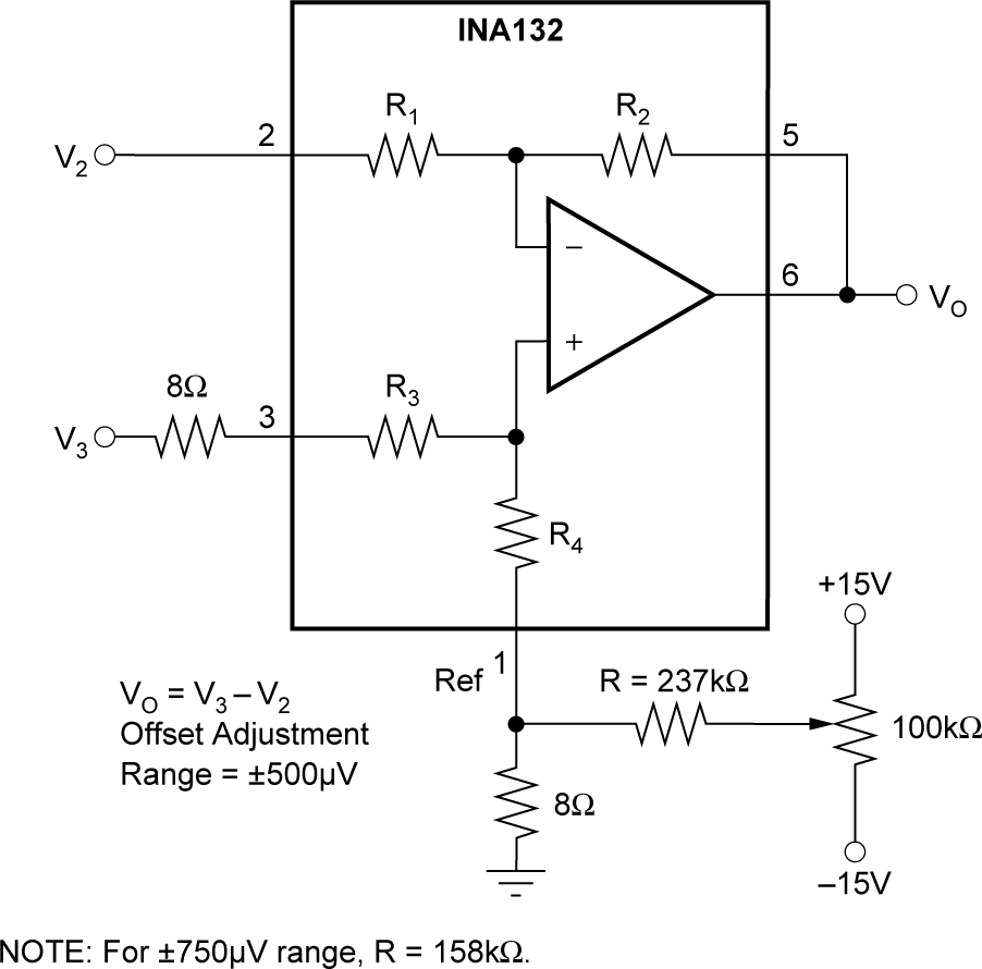
The INA132 is laser trimmed for low offset voltage and drift. Most applications require no external offset adjustment. Figure 6-2 shows an optional circuit for trimming the output offset voltage. The output is referred to the output reference terminal (pin 1), which is normally grounded. A voltage applied to the Ref terminal is summed with the output signal, and can be used to null offset voltage. Ensure that the source impedance of a signal applied to the Ref terminal is less than 8Ω to maintain good common-mode rejection. To maintain low impedance at the Ref terminal, the trim voltage can be buffered with an op amp, such as the OPA177.
 Figure 6-2 Offset Adjustment.