JAJSDR4C August   2017  – May 2019 INA1650-Q1 , INA1651-Q1

PRODUCTION DATA.  

  1. 特長
  2. アプリケーション
    1.     簡略化された内部回路図
  3. 概要
    1.     CMRRヒストグラム(5746チャネル)
  4. 改訂履歴
  5. Pin Configuration and Functions
    1.     Pin Functions: INA1650-Q1
    2.     Pin Functions: INA1651-Q1
  6. Specifications
    1. 6.1 Absolute Maximum Ratings
    2. 6.2 ESD Ratings
    3. 6.3 Recommended Operating Conditions
    4. 6.4 Thermal Information
    5. 6.5 Electrical Characteristics:
    6. 6.6 Typical Characteristics
  7. Detailed Description
    1. 7.1 Overview
    2. 7.2 Functional Block Diagram
    3. 7.3 Feature Description
      1. 7.3.1 Audio Signal Path
      2. 7.3.2 Supply Divider
      3. 7.3.3 EMI Rejection
      4. 7.3.4 Electrical Overstress
      5. 7.3.5 Thermal Shutdown
    4. 7.4 Device Functional Modes
      1. 7.4.1 Single-Supply Operation
  8. Application and Implementation
    1. 8.1 Application Information
      1. 8.1.1 Input Common-Mode Range
      2. 8.1.2 Common-Mode Input Impedance
      3. 8.1.3 Start-Up Time in Single-Supply Applications
      4. 8.1.4 Input AC Coupling
      5. 8.1.5 Supply Divider Capacitive Loading
    2. 8.2 Typical Applications
      1. 8.2.1 Line Receiver for Differential Audio Signals in a Split-Supply System
        1. 8.2.1.1 Design Requirements
        2. 8.2.1.2 Detailed Design Procedure
        3. 8.2.1.3 Application Curves
      2. 8.2.2 Two-Channel Microphone Input for Automotive Infotainment Systems
      3. 8.2.3 TRS Audio Interface in Single-Supply Applications
  9. Power Supply Recommendations
  10. 10Layout
    1. 10.1 Layout Guidelines
    2. 10.2 Layout Example
  11. 11デバイスおよびドキュメントのサポート
    1. 11.1 デバイス・サポート
      1. 11.1.1 開発サポート
        1. 11.1.1.1 TINA-TI(無料のダウンロード・ソフトウェア)
        2. 11.1.1.2 TI Precision Designs
    2. 11.2 ドキュメントのサポート
      1. 11.2.1 関連資料
    3. 11.3 ドキュメントの更新通知を受け取る方法
    4. 11.4 コミュニティ・リソース
    5. 11.5 商標
    6. 11.6 静電気放電に関する注意事項
    7. 11.7 Glossary
  12. 12メカニカル、パッケージ、および注文情報

パッケージ・オプション

メカニカル・データ(パッケージ|ピン)
サーマルパッド・メカニカル・データ
発注情報

Supply Divider

The INA165x-Q1 have an integrated supply-divider circuit that biases the input common-mode voltage and output reference voltage to the halfway point between the applied power supply voltages. The nominal output voltage of the supply divider circuit is shown in Equation 2:

Equation 2. INA1650-Q1 INA1651-Q1 FBD_eq_002.gif

Figure 40 illustrates the internal topology of the supply-divider circuit. The supply divider consists of two 500-kΩ resistors connected between the VCC and VEE pins of the INA165x-Q1. The noninverting input of a buffer amplifier is connected to the midpoint of the voltage divider that is formed by the 500-kΩ resistors. The buffer amplifier provides a low-impedance output that is required to bias the REF pins without degrading the CMRR. For dual-supply applications where the supply divider circuit is not used, no connection is required for the VMID(IN) or VMID(OUT) pins.
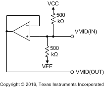
INA1650-Q1 INA1651-Q1 FD_D002.gifFigure 40. Internal Supply Divider Circuit