JAJSCM3E August 2006 – January 2021 INA193A-Q1 , INA194A-Q1 , INA195A-Q1 , INA196A-Q1 , INA197A-Q1 , INA198A-Q1
PRODUCTION DATA
- 1 特長
- 2 アプリケーション
- 3 概要
- 4 Revision History
- 5 Pin Configuration and Functions
- 6 Specifications
- 7 Detailed Description
- 8 Application and Implementation
- 9 Power Supply Recommendations
- 10Layout
- 11Device and Documentation Support
- 12Mechanical, Packaging, and Orderable Information
7.4.2.1 Normal Case 1: VSENSE ≥ 20 mV, VCM ≥ VS
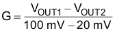
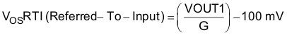
This region of operation provides the highest accuracy. Here, the input offset voltage is characterized and measured using a two-step method. First, the gain is determined by (Equation 2).
where
- VOUT1 = Output voltage with VSENSE = 100 mV
- VOUT2 = Output voltage with VSENSE = 20 mV
The offset voltage is then measured at VSENSE = 100 mV and referred to the input (RTI) of the current shunt monitor, as shown in (Equation 3).
In GUID-DB3CDEB3-CF31-4CD4-A2A4-13992281C45A.html#GUID-DB3CDEB3-CF31-4CD4-A2A4-13992281C45A, the Output Error vs Common Mode Voltage curve shows the highest accuracy for the this region of operation. In this plot, VS = 12 V; for VCM ≥ 12 V, the output error is at its minimum. This case is also used to create the VSENSE ≥ 20 mV output specifications in the Electrical Characteristics table.