JAJSCM0C April 2011 – April 2016 INA200-Q1 , INA201-Q1 , INA202-Q1
PRODUCTION DATA.
- 1 特長
- 2 アプリケーション
- 3 概要
- 4 改訂履歴
- 5 Device Comparison Table
- 6 Pin Configuration and Functions
- 7 Specifications
- 8 Parameter Measurement Information
- 9 Detailed Description
- 10Application Information
- 11Power Supply Recommendations
- 12Layout
- 13デバイスおよびドキュメントのサポート
- 14メカニカル、パッケージ、および注文情報
9 Detailed Description
9.1 Overview
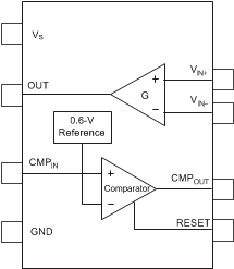
The INA20x-Q1 current-shunt monitors operate over a wide common-mode voltage range (–16 V to +80 V). These devices integrate an open-drain comparator with an internal 0.6-V reference at the negative input. Use external dividers from the output of the current shunt monitor to the positive input of the comparator to set the positive input for overcurrent detection. The comparator includes a latching capability, but can also be made transparent by grounding (or floating) the RESET pin.
9.2 Functional Block Diagram

9.3 Feature Description
9.3.1 Comparator
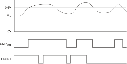
The INA200-Q1, INA201-Q1, and INA202-Q1 devices incorporate an open-drain comparator. This comparator typically has 2 mV of offset and a 1.3 μs (typical) response time. The RESET pin latches and resets the output of the comparator; see Figure 26.
 Figure 26. Comparator Latching Capability
9.3.2 Output Voltage Range
The output of the INA20x-Q1 is accurate within the output voltage swing range set by the power supply pin, VS. Best illustration of this performance occurs when using the INA202-Q1 (gain-of-100 version), where a 100-mV full-scale input from the shunt resistor requires an output voltage swing of 10 V, and a power-supply voltage sufficient to achieve 10 V on the output.
9.4 Device Functional Modes
The INA20x-Q1 have a single functional mode and are operational when the power-supply voltage is greater than 2.7 V. The common-mode voltage must be between –16 V and +80 V. The maximum power supply voltage for the INA20x-Q1 is 18 V.