JAJSKH9C March   2012  – January 2021 INA282-Q1 , INA283-Q1 , INA284-Q1 , INA285-Q1 , INA286-Q1

PRODUCTION DATA  

  1. 特長
  2. アプリケーション
  3. 概要
  4. Revision History
  5. Pin Configuration and Functions
  6. Specifications
    1. 6.1 Absolute Maximum Ratings
    2. 6.2 ESD Ratings
    3. 6.3 Recommended Operating Conditions
    4. 6.4 Thermal Information
    5. 6.5 Electrical Characteristics
    6. 6.6 Typical Characteristics
  7. Detailed Description
    1. 7.1 Overview
    2. 7.2 Functional Block Diagram
    3. 7.3 Feature Description
      1. 7.3.1 Selecting RS
      2. 7.3.2 Effective Bandwidth
      3. 7.3.3 Transient Protection
    4. 7.4 Device Functional Modes
      1. 7.4.1 Reference Pin Connection Options
        1. 7.4.1.1 Unidirectional Operation
          1. 7.4.1.1.1 Ground Referenced Output
          2. 7.4.1.1.2 V+ Referenced Output
        2. 7.4.1.2 Bidirectional Operation
          1. 7.4.1.2.1 External Reference Output
          2. 7.4.1.2.2 Splitting the Supply
          3. 7.4.1.2.3 Splitting an External Reference
      2. 7.4.2 Shutdown
      3. 7.4.3 Extended Negative Common-Mode Range
      4. 7.4.4 Calculating Total Error
        1. 7.4.4.1 Example 1 INA282-Q1
        2. 7.4.4.2 Example 2 INA286-Q1
  8. Application and Implementation
    1. 8.1 Application Information
      1. 8.1.1 Basic Connections
    2. 8.2 Typical Applications
      1. 8.2.1 Current Summing
        1. 8.2.1.1 Design Requirements
        2. 8.2.1.2 Detailed Design Procedures
        3. 8.2.1.3 Application Curve
      2. 8.2.2 Current Differencing
        1. 8.2.2.1 Design Requirements
        2. 8.2.2.2 Detailed Design Procedure
        3. 8.2.2.3 Application Curve
  9. Power Supply Recommendations
  10. 10Layout
    1. 10.1 Layout Guidelines
    2. 10.2 Layout Example
  11. 11Device and Documentation Support
    1. 11.1 ドキュメントの更新通知を受け取る方法
    2. 11.2 サポート・リソース
    3. 11.3 Trademarks
    4. 11.4 静電気放電に関する注意事項
  12. 12用語集
  13. 13Mechanical, Packaging, and Orderable Information

パッケージ・オプション

メカニカル・データ(パッケージ|ピン)
サーマルパッド・メカニカル・データ
発注情報

Reference Pin Connection Options

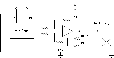
#SBOS4853533 illustrates a test circuit for reference divider accuracy. The output of the INA28x-Q1 can be connected for unidirectional or bidirectional operation. Neither the REF1 pin nor the REF2 pin may be connected to any voltage source lower than GND or higher than V+, and that the effective reference voltage (REF1 + REF2)/2 must be 9 V or less. This parameter means that the V+ reference output connection shown in GUID-C3990AF6-8976-4FE8-BB7C-5D6225FC8054.html#SBOS4858668 is not allowed for V+ greater than 9 V. However, the split-supply reference connection shown in GUID-3289C24F-9DE9-4FDC-A544-EC39001DE851.html#SBOS4854503 is allowed for all values of V+ up to 18 V.
GUID-4ACA9221-3149-4167-91EB-ACD20F1D2096-low.gif
Reference divider accuracy is determined by measuring the output with the reference voltage applied to alternate reference resistors, and calculating a result such that the amplifier offset is cancelled in the final measurement.
Figure 7-1 Test Circuit for Reference Divider Accuracy