JAJSE68 November 2017 INA317
PRODUCTION DATA.
- 1 特長
- 2 アプリケーション
- 3 概要
- 4 改訂履歴
- 5 Pin Configuration and Functions
- 6 Specifications
- 7 Detailed Description
- 8 Application and Implementation
- 9 Power Supply Recommendations
- 10Layout
- 11デバイスおよびドキュメントのサポート
- 12メカニカル、パッケージ、および注文情報
10 Layout
10.1 Layout Guidelines
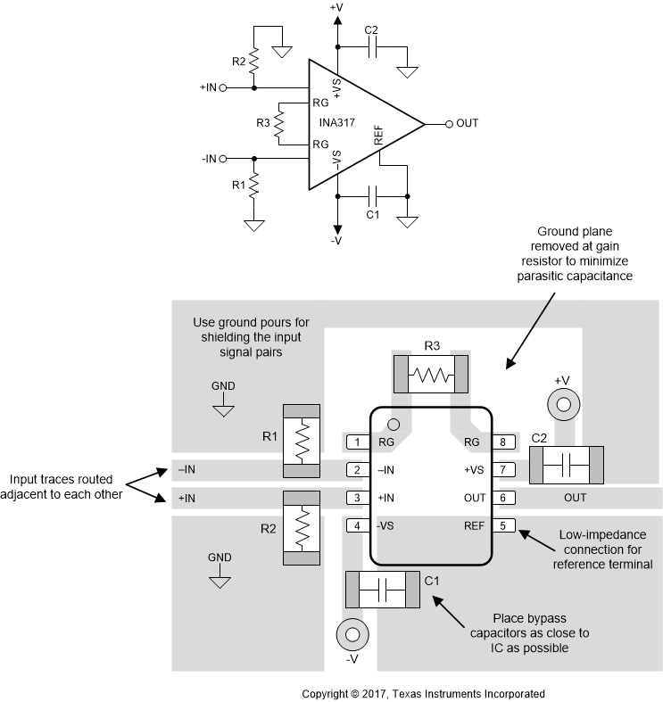
TI recommends paying attention to good layout practices. Keep traces short and use a printed-circuit-board (PCB) ground plane with surface-mount components placed as close to the device pins as possible. Place a 0.1-µF bypass capacitor as close as possible the supply pins. Apply these guidelines throughout the analog circuit to improve performance and reduce electromagnetic interference (EMI) susceptibility.
Instrumentation amplifiers vary in the susceptibility to radio-frequency interference (RFI). RFI is identified as a variation in offset voltage or DC signal levels with changes in the interfering RF signal. The INA317 device is designed to minimize susceptibility to RFI by incorporating passive RC filters with an 8-MHz corner frequency at the VIN+ and VIN– inputs. As a result, the INA317 device demonstrates low sensitivity compared to previous generation devices. However, strong RF fields can cause varied offset levels and may require additional shielding.
10.2 Layout Example
 Figure 40. INA317 Layout