JAJSEX6B December   2017  – October 2019 INA381

PRODUCTION DATA.  

  1. 特長
  2. アプリケーション
  3. 概要
    1.     Device Images
      1.      代表的なアプリケーション
  4. 改訂履歴
  5. 概要(続き)
  6. Pin Configuration and Functions
    1.     Pin Functions
  7. Specifications
    1. 7.1 Absolute Maximum Ratings
    2. 7.2 ESD Ratings
    3. 7.3 Recommended Operating Conditions
    4. 7.4 Thermal Information
    5. 7.5 Electrical Characteristics
    6. 7.6 Typical Characteristics
  8. Detailed Description
    1. 8.1 Overview
    2. 8.2 Functional Block Diagram
    3. 8.3 Feature Description
      1. 8.3.1 Wide Input Common-Mode Voltage Range
      2. 8.3.2 Precise Low-Side Current Sensing
      3. 8.3.3 High Bandwidth and Slew Rate
      4. 8.3.4 Alert Output
      5. 8.3.5 Adjustable Overcurrent Threshold
      6. 8.3.6 Comparator Hysteresis
    4. 8.4 Device Functional Modes
      1. 8.4.1 Alert Modes
        1. 8.4.1.1 Transparent Output Mode
        2. 8.4.1.2 Latch Output Mode
  9. Applications and Implementation
    1. 9.1 Application Information
      1. 9.1.1 Select a Current-Sensing Resistor
        1. 9.1.1.1 Select a Current-Sensing Resistor: Example
      2. 9.1.2 Increase Comparator Hysteresis
      3. 9.1.3 Operation With Common-Mode Transients Greater Than 26 V
      4. 9.1.4 Input Filtering
    2. 9.2 Typical Applications
      1. 9.2.1 Bidirectional Window Comparator
        1. 9.2.1.1 Design Requirements
        2. 9.2.1.2 Detailed Design Procedure
        3. 9.2.1.3 Application Curve
      2. 9.2.2 Solenoid Low-Side Current Sensing
        1. 9.2.2.1 Design Requirements
        2. 9.2.2.2 Detailed Design Procedure
        3. 9.2.2.3 Application Curve
  10. 10Power Supply Recommendations
  11. 11Layout
    1. 11.1 Layout Guidelines
    2. 11.2 Layout Example
  12. 12デバイスおよびドキュメントのサポート
    1. 12.1 ドキュメントのサポート
      1. 12.1.1 関連資料
    2. 12.2 ドキュメントの更新通知を受け取る方法
    3. 12.3 サポート・リソース
    4. 12.4 商標
    5. 12.5 静電気放電に関する注意事項
    6. 12.6 Glossary
  13. 13メカニカル、パッケージ、および注文情報

パッケージ・オプション

デバイスごとのパッケージ図は、PDF版データシートをご参照ください。

メカニカル・データ(パッケージ|ピン)
  • DGS|10
  • DSG|8
サーマルパッド・メカニカル・データ
発注情報

Alert Output

The ALERT pin is an active-low, open-drain output pulls low when the input conditions are out-of-range. This open-drain output pin is recommended to include a 10-kΩ pullup resistor to the supply voltage. This open-drain pin can be pulled up to a voltage beyond the supply voltage, VS, but must not exceed 5.5 V.

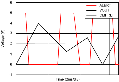
Figure 41 shows the alert output response of the internal comparator. When the output voltage of the amplifier is less than the reference voltage set on CMPREF, the comparator output is in the default high state. When the amplifier output voltage exceeds the reference voltage set at the CMPREF pin, the comparator output becomes active and pulls low. This active low output indicates that the measured signal at the amplifier input has exceeded the programmed threshold level, indicating an overcurrent or out-of-range condition has occurred. See the Alert Modes section for more information about how to set the alert output behavior.
INA381 Fig3OvercurrResponse.gifFigure 41. Overcurrent Alert Response