SLLS629L January 2006 – October 2015 ISO721 , ISO721M , ISO722 , ISO722M
PRODUCTION DATA.
- 1 Features
- 2 Applications
- 3 Description
- 4 Revision History
- 5 Device Comparison Table
- 6 Pin Configuration and Functions
-
7 Specifications
- 7.1 Absolute Maximum Ratings
- 7.2 ESD Ratings
- 7.3 Recommended Operating Conditions
- 7.4 Thermal Information
- 7.5 Electrical Characteristics, 5 V
- 7.6 Electrical Characteristics, 5 V, 3.3 V
- 7.7 Electrical Characteristics, 3.3 V, 5 V
- 7.8 Electrical Characteristics, 3.3 V
- 7.9 Power Dissipation
- 7.10 Switching Characteristics, 5 V
- 7.11 Switching Characteristics, 5 V, 3.3 V
- 7.12 Switching Characteristics, 3.3 V, 5 V
- 7.13 Switching Characteristics, 3.3 V
- 7.14 Typical Characteristics
- 8 Parameter Measurement Information
- 9 Detailed Description
- 10Application and Implementation
- 11Power Supply Recommendations
- 12Layout
- 13Device and Documentation Support
- 14Mechanical, Packaging, and Orderable Information
10 Application and Implementation
NOTE
Information in the following applications sections is not part of the TI component specification, and TI does not warrant its accuracy or completeness. TI’s customers are responsible for determining suitability of components for their purposes. Customers should validate and test their design implementation to confirm system functionality.
10.1 Application Information
The ISO72x devices use single-ended TTL or CMOS-logic-switching technology. The supply voltage range of the devices is from 3 V to 5.5 V for both supplies, VCC1 and VCC2. When designing with digital isolators, due to the single-ended design structure, digital isolators do not conform to any specific interface standard and are only intended for isolating single-ended CMOS or TTL digital signal lines. The isolator is typically placed between the data controller (μC or UART), and a data converter or a line transceiver, regardless of the interface type or standard.
10.2 Typical Application
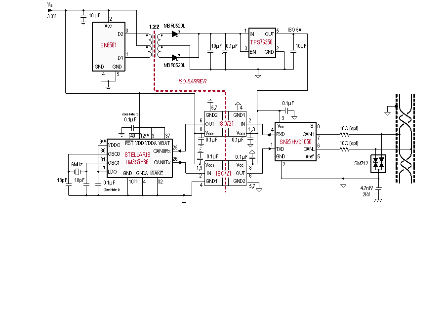
The ISO721 device can be used with Texas Instruments’ microcontroller, CAN transceiver, transformer driver, and low-dropout voltage regulator to create an Isolated CAN Interface as shown in Figure 18.

10.2.1 Design Requirements
Unlike optocouplers which need external components to improve performance and provide bias (or limit current), the ISO72x devices need only two external bypass capacitors to operate.
10.2.2 Detailed Design Procedure
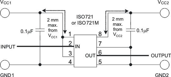
Typical ISO721 circuit hook-up is shown in Figure 19.
The ISO72x isolators have the same functional pinout as those of most other vendors as shown in Figure 20, and they are often pin-for-pin drop-in replacements. The notable differences in the products are propagation delay, signaling rate, power consumption, and transient protection rating. Table 3 is used as a guide for replacing other isolators with the ISO72x family of single channel isolators.
 Figure 20. Pin Cross Reference
Table 3. Cross Reference
| ISOLATOR | PIN 1 | PIN 2 | PIN 3 | PIN 4 | PIN 5 | PIN 6 | PIN 7 | PIN 8 | |
|---|---|---|---|---|---|---|---|---|---|
| ISO721 OR ISO721M |
ISO722 OR ISO722M |
||||||||
| ISO721(1)(2) | VCC1 | IN | VCC1 | GND1 | GND2 | OUT | GND2 | EN | VCC2 |
| ADuM1100(1)(2) | VDD1 | VI | VDD1 | GND1 | GND2 | VO | GND2 | VDD2 | |
| HCPL-xxxx | VDD1 | VI | *Leave Open(3) | GND1 | GND2 | VO | NC(5) | VDD2 | |
| IL710 | VDD1 | VI | NC(4) | GND1 | GND2 | VO | V OE | VDD2 | |
10.2.3 Application Curves
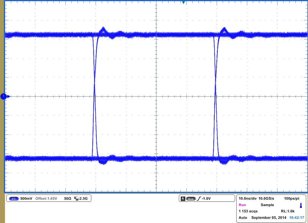
 Figure 21. ISO721M Eye Diagram at 25 Mbps,
3.3 V and 25°C
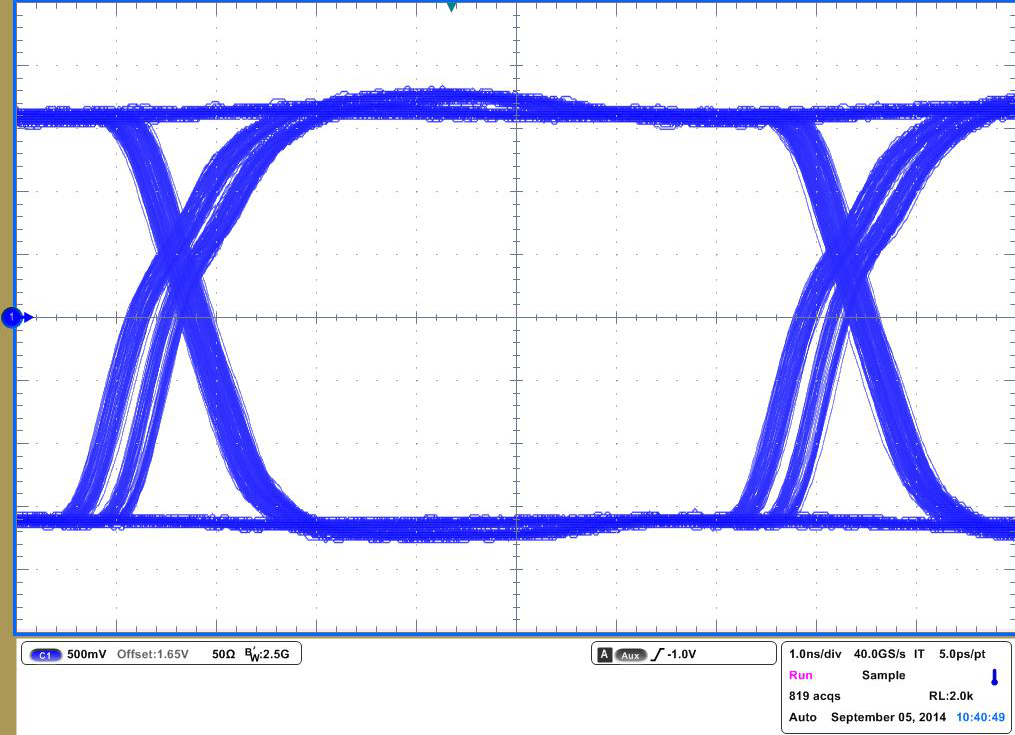
 Figure 22. ISO721M Eye Diagram at 150 Mbps,
3.3 V and 25°C
