JAJSCT7A March 2016 – August 2016 ISO7820LL , ISO7821LL
PRODUCTION DATA.
- 1 特長
- 2 アプリケーション
- 3 概要
- 4 改訂履歴
- 5 Pin Configuration and Functions
-
6 Specifications
- 6.1 Absolute Maximum Ratings
- 6.2 ESD Ratings
- 6.3 Recommended Operating Conditions
- 6.4 Thermal Information
- 6.5 Power Ratings
- 6.6 Insulation Specifications
- 6.7 Safety-Related Certifications
- 6.8 Safety Limiting Values
- 6.9 DC Electrical Characteristics
- 6.10 DC Supply Current Characteristics
- 6.11 Switching Characteristics
- 6.12 Insulation Characteristics Curves
- 6.13 Typical Characteristics
- 7 Parameter Measurement Information
- 8 Detailed Description
- 9 Application and Implementation
- 10Power Supply Recommendations
- 11Layout
- 12デバイスおよびドキュメントのサポート
- 13メカニカル、パッケージ、および注文情報
パッケージ・オプション
メカニカル・データ(パッケージ|ピン)
サーマルパッド・メカニカル・データ
- DW|16
発注情報
5 Pin Configuration and Functions
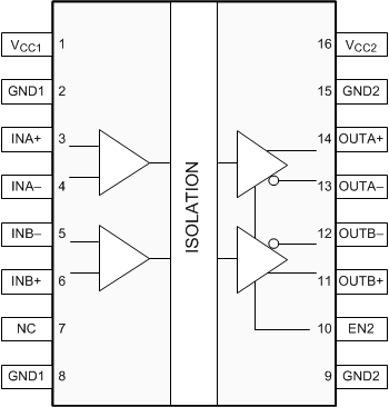
ISO7820LL DW and DWW Packages
16-Pin SOIC
Top View

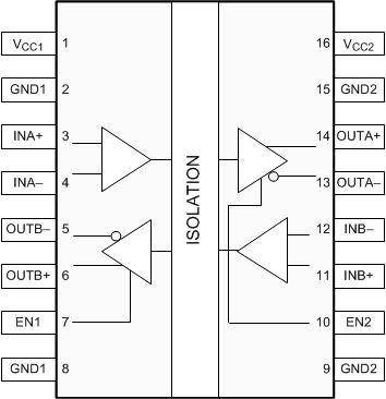
ISO7821LL DW and DWW Packages
16-Pin SOIC
Top View

Pin Functions
| PIN | I/O | DESCRIPTION | ||
|---|---|---|---|---|
| NAME | NO. | |||
| ISO7820LL | ISO7821LL | |||
| EN1 | — | 7 | I | Output enable 1. Output pins on side 1 are enabled when EN1 is high or open and in high impedance state when EN1 is low. |
| EN2 | 10 | 10 | I | Output enable 2. Output pins on side 2 are enabled when EN2 is high or open and in high impedance state when EN2 is low. |
| GND1 | 2 | 2 | — | Ground connection for VCC1 |
| 8 | 8 | |||
| GND2 | 9 | 9 | — | Ground connection for VCC2 |
| 15 | 15 | |||
| INA+ | 3 | 3 | I | Positive differential input, channel A |
| INA– | 4 | 4 | I | Negative differential input, channel A |
| INB+ | 6 | 11 | I | Positive differential input, channel B |
| INB– | 5 | 12 | I | Negative differential input, channel B |
| NC | 7 | — | — | Not connected |
| OUTA+ | 14 | 14 | O | Positive differential output, channel A |
| OUTA– | 13 | 13 | O | Negative differential output, channel A |
| OUTB+ | 11 | 6 | O | Positive differential output, channel B |
| OUTB– | 12 | 5 | O | Negative differential output, channel B |
| VCC1 | 1 | 1 | — | Power supply, side 1, VCC1 |
| VCC2 | 16 | 16 | — | Power supply, side 2, VCC2 |