JAJSUC2B December   2015  – April 2024 LDC0851

PRODUCTION DATA  

  1.   1
  2. 特長
  3. アプリケーション
  4. 概要
  5. Pin Configuration and Functions
  6. Specifications
    1. 5.1 Absolute Maximum Ratings
    2. 5.2 ESD Ratings
    3. 5.3 Recommended Operating Conditions
    4. 5.4 Thermal Information
    5. 5.5 Electrical Characteristics
    6. 5.6 Interface Voltage Levels
    7. 5.7 Timing Requirements
    8. 5.8 Typical Characteristics
  7. Detailed Description
    1. 6.1 Overview
    2. 6.2 Functional Block Diagram
    3. 6.3 Feature Description
      1. 6.3.1 Basic Operation Mode
      2. 6.3.2 Threshold Adjust Mode
      3. 6.3.3 Setting the Threshold Adjust Values
      4. 6.3.4 Hysteresis
      5. 6.3.5 Conversion Time
      6. 6.3.6 Power-Up Conditions
    4. 6.4 Device Functional Modes
      1. 6.4.1 Shutdown Mode
      2. 6.4.2 Active Mode
  8. Application and Implementation
    1. 7.1 Application Information
      1. 7.1.1 Sensor Design
        1. 7.1.1.1 Sensor Frequency
        2. 7.1.1.2 Sensor Design Procedure
    2. 7.2 Typical Application
      1. 7.2.1 Event Counting
        1. 7.2.1.1 Design Requirements
        2. 7.2.1.2 Detailed Design Procedure
        3. 7.2.1.3 Application Curves
      2. 7.2.2 Coarse Position Sensing
        1. 7.2.2.1 Design Requirements
        2. 7.2.2.2 Detailed Design Procedure
        3. 7.2.2.3 Application Curves
      3. 7.2.3 Low Power Operation
        1. 7.2.3.1 Design Requirements
        2. 7.2.3.2 Detailed Design Procedure
        3. 7.2.3.3 Application Curves
    3. 7.3 Power Supply Recommendations
    4. 7.4 Layout
      1. 7.4.1 Layout Guidelines
      2. 7.4.2 Layout Example
        1. 7.4.2.1 Side by Side Coils
        2. 7.4.2.2 Stacked Coils
  9. Device and Documentation Support
    1. 8.1 Device Support
      1. 8.1.1 Development Support
    2. 8.2 Documentation Support
      1. 8.2.1 Related Documentation
    3. 8.3 サポート・リソース
    4. 8.4 Trademarks
    5. 8.5 静電気放電に関する注意事項
    6. 8.6 用語集
  10. Revision History
  11. 10Mechanical, Packaging, and Orderable Information

パッケージ・オプション

メカニカル・データ(パッケージ|ピン)
サーマルパッド・メカニカル・データ
発注情報

Power Supply Recommendations

A 0.1 µF capacitor should be used to bypass VDD. If multiple bypass capacitors are used in the system, then the smallest value capacitor should be placed as close as possible to the VDD pin. A ground plane is recommended to connect both the ground and the Die Attach Pad (DAP). If the supply ramp rate must be faster than 4.2 mV/µs the enable pin (EN) may be tied directly to VDD as shown in Figure 7-8.
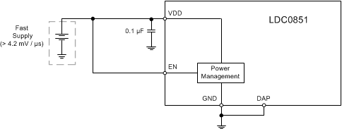
LDC0851 Supply Connections for
                        Fast Ramp Rate Figure 7-8 Supply Connections for Fast Ramp Rate

For supply ramp rates slower than 4.2 mV/µs, an RC low pass filter must be added to the enable input (EN) as shown in Figure 7-9. Alternatively, the EN pin may be tied to a nanotimer or microcontroller to wake up the LDC0851 after VDD has ramped to its nominal value.
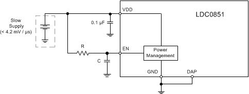
LDC0851 Supply Connections for
                        Slow Ramp Rate Figure 7-9 Supply Connections for Slow Ramp Rate

For applications that require low power, the EN pin may toggled with a GPIO or nanotimer to duty cycle the device and achieve ultra-low power consumption. Although the device may be power cycled to achieve a similar effect, some systems may not have a clean GPIO to supply the LDC0851 or the filtering on the supply may add a time constant delay which can make the use of the EN pin much more efficient and desirable for duty cycled applications. Refer to Low Power Operation for a detailed design example.