JAJSDC7 June   2017 LM10-MIL

PRODUCTION DATA.  

  1. 特長
  2. アプリケーション
  3. 概要
  4. 改訂履歴
  5. Pin Configuration and Functions
  6. Specifications
    1. 6.1 Absolute Maximum Ratings
    2. 6.2 Recommended Operating Conditions
    3. 6.3 Thermal Information
    4. 6.4 Electrical Characteristics
    5. 6.5 Typical Characteristics
      1. 6.5.1 Typical Characteristics (Op Amp)
      2. 6.5.2 Typical Characteristics (Reference)
  7. Detailed Description
    1. 7.1 Overview
    2. 7.2 Functional Block Diagram
    3. 7.3 Feature Description
      1. 7.3.1 Operating Characteristics
      2. 7.3.2 Common-Mode Voltage Range
      3. 7.3.3 Operational Amplifier
      4. 7.3.4 Voltage Reference
    4. 7.4 Device Functional Modes
      1. 7.4.1 Floating Mode
      2. 7.4.2 Linear Operation
  8. Application and Implementation
    1. 8.1 Application Information
    2. 8.2 Typical Application
      1. 8.2.1 Design Requirements
      2. 8.2.2 Detailed Design Procedure
      3. 8.2.3 Application Curve
    3. 8.3 System Examples
      1. 8.3.1 Operational Amplifier Offset Adjustment
      2. 8.3.2 Positive Regulators
      3. 8.3.3 Reference and Internal Regulator
  9. Power Supply Recommendations
  10. 10Layout
    1. 10.1 Layout Guidelines
    2. 10.2 Layout Example
  11. 11デバイスおよびドキュメントのサポート
    1. 11.1 デバイス・サポート
      1. 11.1.1 デバイスの関連用語
        1. 11.1.1.1 用語の定義
    2. 11.2 ドキュメントのサポート
      1. 11.2.1 関連資料
    3. 11.3 コミュニティ・リソース
    4. 11.4 商標
    5. 11.5 静電気放電に関する注意事項
    6. 11.6 Glossary
  12. 12メカニカル、パッケージ、および注文情報

パッケージ・オプション

メカニカル・データ(パッケージ|ピン)
サーマルパッド・メカニカル・データ
発注情報

Layout

Layout Guidelines

For best operational performance of the device, good printed-circuit board (PCB) layout practices are recommended. Low-loss, 0.1-uF bypass capacitors should be connected between each supply pin and ground, placed as close to the device as possible. A single bypass capacitor from V+ to ground is applicable to single-supply applications.

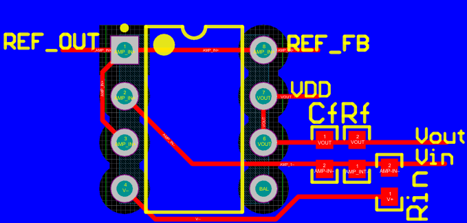
Layout Example

LM10-MIL snosbh4_layout_example_board_layer.gif Figure 72. Layout Example