SNVS589N September 2008 – November 2014 LM22671 , LM22671-Q1
PRODUCTION DATA.
- 1 Features
- 2 Applications
- 3 Description
- 4 Revision History
- 5 Pin Configuration and Functions
- 6 Specifications
- 7 Detailed Description
- 8 Application and Implementation
- 9 Power Supply Recommendations
- 10Layout
- 11Device and Documentation Support
- 12Mechanical, Packaging, and Orderable Information
5 Pin Configuration and Functions
HSOP Package
8-Pin
Top View
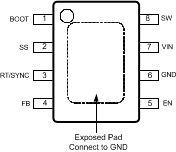
Pin Functions
| PIN | TYPE | DESCRIPTION | APPLICATION INFORMATION | |
|---|---|---|---|---|
| NAME | NO. | |||
| BOOT | 1 | I | Bootstrap input | Provides the gate voltage for the high side NFET. |
| EN | 5 | I | Precision enable pin | Used to control regulator start-up and shut-down. See the Precision Enable and UVLO section of data sheet. |
| EP | EP | — | Exposed Pad | Connect to ground. Provides thermal connection to PCB. See the Application and Implementation. |
| FB | 4 | Feedback pin | Feedback input to regulator. | |
| GND | 6 | — | System ground | System ground pin. |
| RT/SYNC | 3 | Oscillator frequency adjust pin or frequency synchronization | Used to control oscillator mode of regulator. See the Switching Frequency Adjustment and Synchronization section of data sheet. | |
| SS | 2 | Soft-start pin | Used to increase soft-start time. See the Soft-Start section of data sheet. | |
| SW | 8 | O | Switch pin | Switching output of regulator. |
| VIN | 7 | I | Source input voltage | Supply input to the regulator. |