JAJSAZ1M February   2013  – October 2020 LM22679 , LM22679-Q1

PRODUCTION DATA  

  1. 特長
  2. アプリケーション
  3. 概要
  4. Revision History
  5. Pin Configuration and Functions
    1.     Pin Functions
  6. Specifications
    1. 6.1 Absolute Maximum Ratings
    2. 6.2 Handling Ratings: LM22679
    3. 6.3 Handling Ratings: LM22679-Q1
    4. 6.4 Recommended Operating Conditions
    5. 6.5 Thermal Information
    6. 6.6 Electrical Characteristics
    7. 6.7 Typical Characteristics
  7. Detailed Description
    1. 7.1 Overview
    2. 7.2 Functional Block Diagram
    3. 7.3 Feature Description
      1. 7.3.1 UVLO
      2. 7.3.2 Soft-Start
      3. 7.3.3 Bootstrap Supply
      4. 7.3.4 Internal Compensation
    4. 7.4 Device Functional Modes
      1. 7.4.1 Shutdown Mode
      2. 7.4.2 Active Mode
      3. 7.4.3 Current Limit
      4. 7.4.4 Current Limit Adjustment
      5. 7.4.5 Thermal Protection
      6. 7.4.6 Duty-Cycle Limits
  8. Application and Implementation
    1. 8.1 Application Information
      1. 8.1.1 Output Voltage Divider Selection
      2. 8.1.2 Power Diode
    2. 8.2 Typical Application
      1. 8.2.1 Typical Buck Regulator Application
        1. 8.2.1.1 Design Requirements
        2. 8.2.1.2 Detailed Design Procedure
          1. 8.2.1.2.1 External Components
          2. 8.2.1.2.2 Inductor
          3. 8.2.1.2.3 Input Capacitor
          4. 8.2.1.2.4 Output Capacitor
          5. 8.2.1.2.5 Bootstrap Capacitor
        3. 8.2.1.3 Application Curve
  9. Power Supply Recommendations
  10. 10Layout
    1. 10.1 Layout Guidelines
    2. 10.2 Layout Example
    3. 10.3 Thermal Considerations
  11. 11Device and Documentation Support
    1. 11.1 Documentation Support
      1. 11.1.1 Related Documentation
    2. 11.2 サポート・リソース
    3. 11.3 ドキュメントの更新通知を受け取る方法
    4. 11.4 Trademarks
    5. 11.5 用語集
    6. 11.6 静電気放電に関する注意事項

パッケージ・オプション

メカニカル・データ(パッケージ|ピン)
サーマルパッド・メカニカル・データ
発注情報

Typical Characteristics

Vin = 12 V, TJ = 25°C (unless otherwise specified)
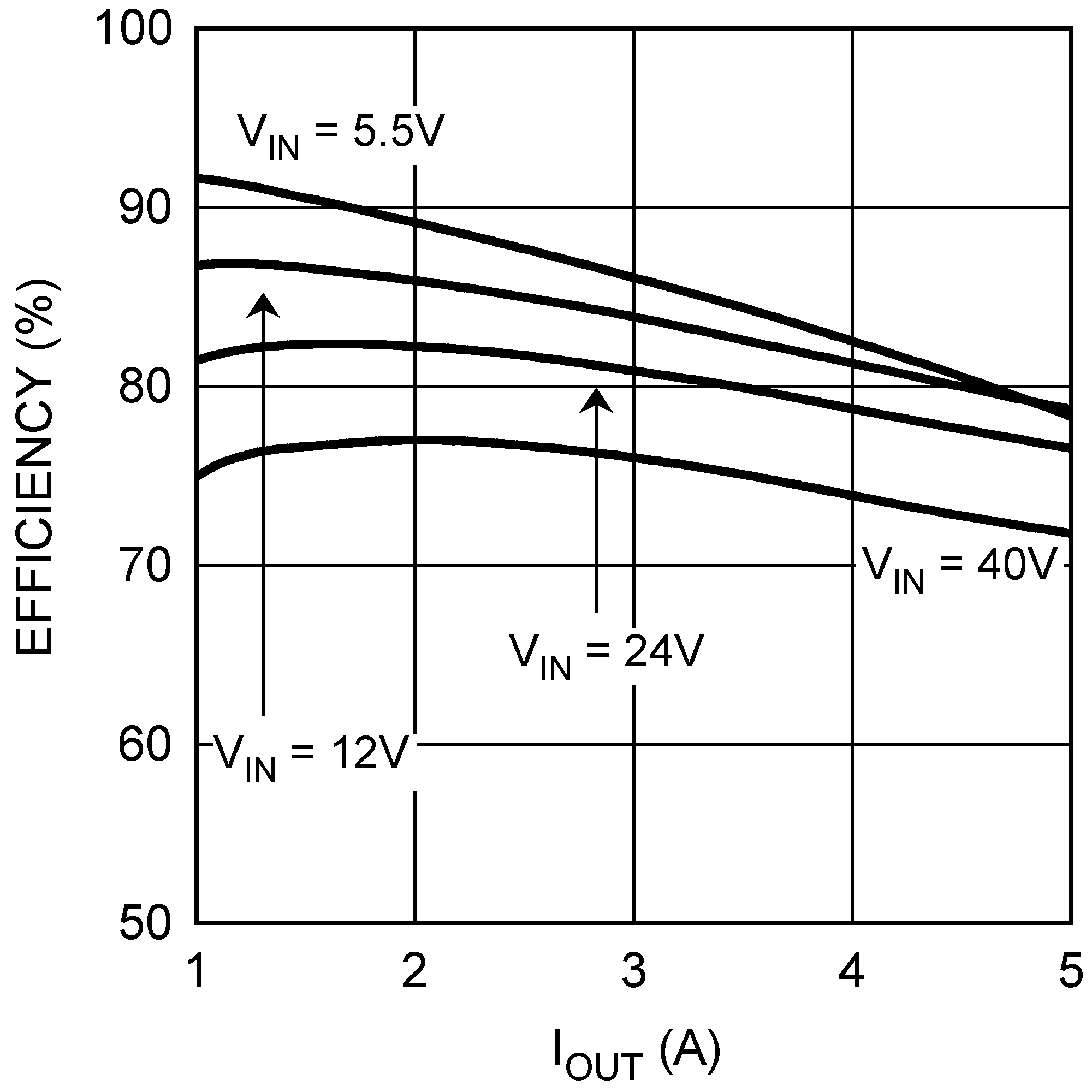
GUID-9EAF593A-0AE7-425F-9CDD-7324AB32748B-low.pngFigure 6-1 Efficiency vs IOUT and VIN (VOUT = 3.3 V)
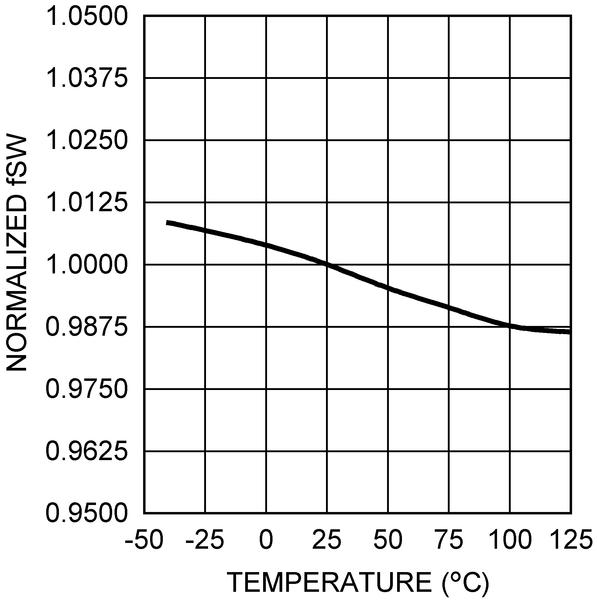
GUID-D24FF2B9-6F13-42D2-97FB-447EA36B3782-low.pngFigure 6-3 Normalized Switching Frequency vs Temperature
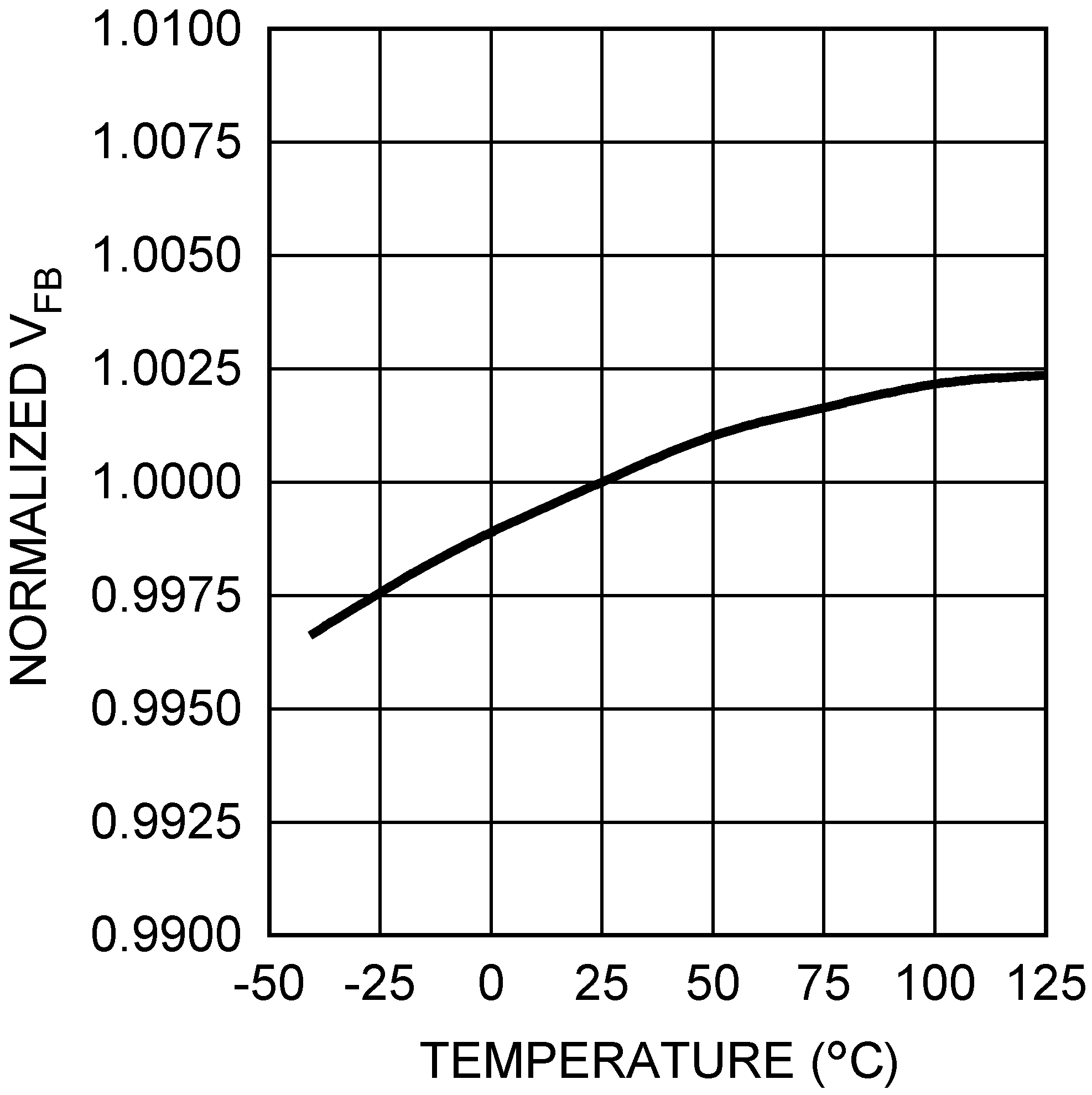
GUID-6B863FDC-00A9-4AD6-84F1-C82CFB76E24A-low.pngFigure 6-5 Normalized Feedback Voltage vs Temperature
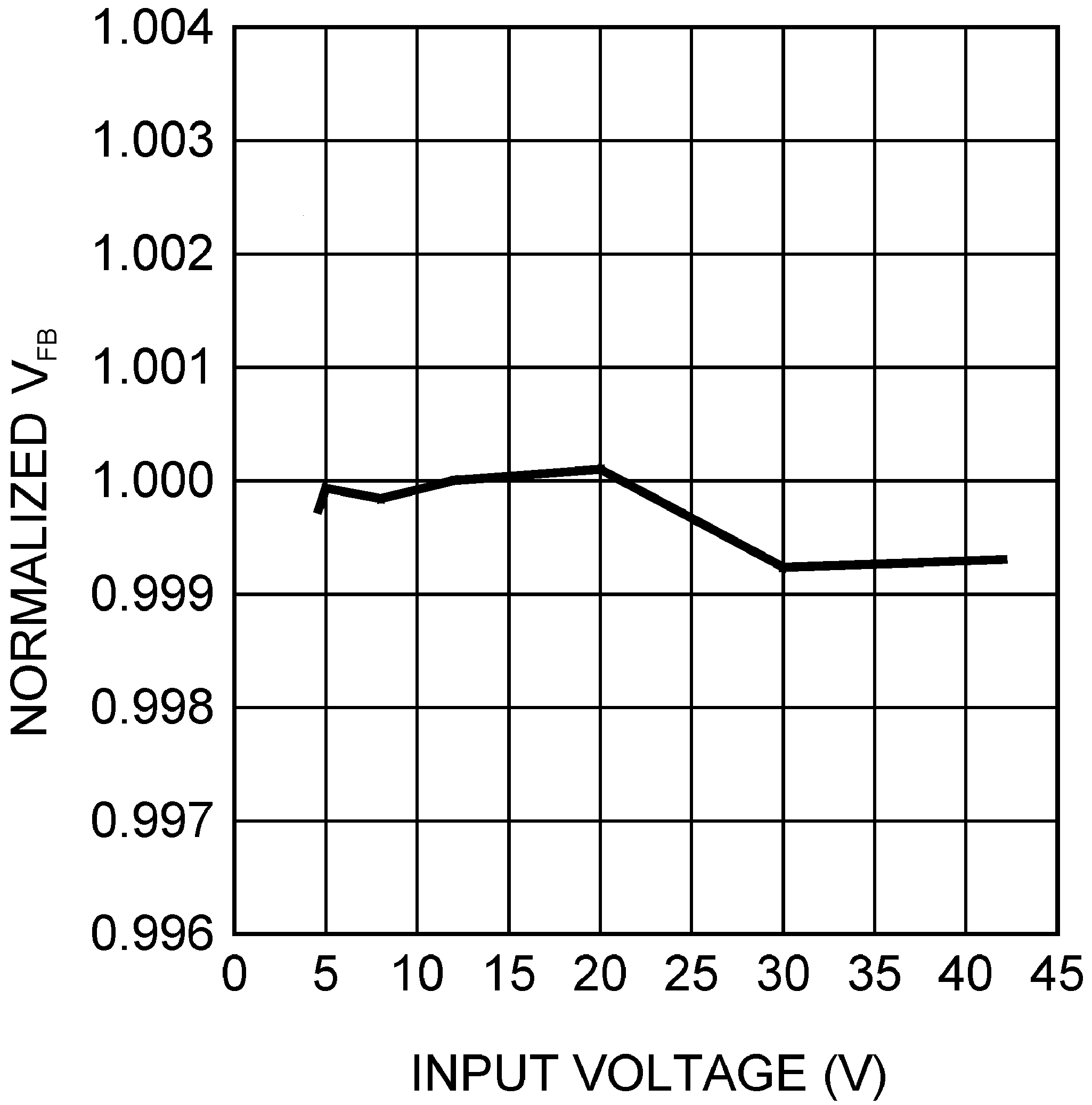
GUID-E3D7A8E2-9E3E-4920-8056-24668A112371-low.pngFigure 6-7 Normalized Feedback Voltage vs Input Voltage
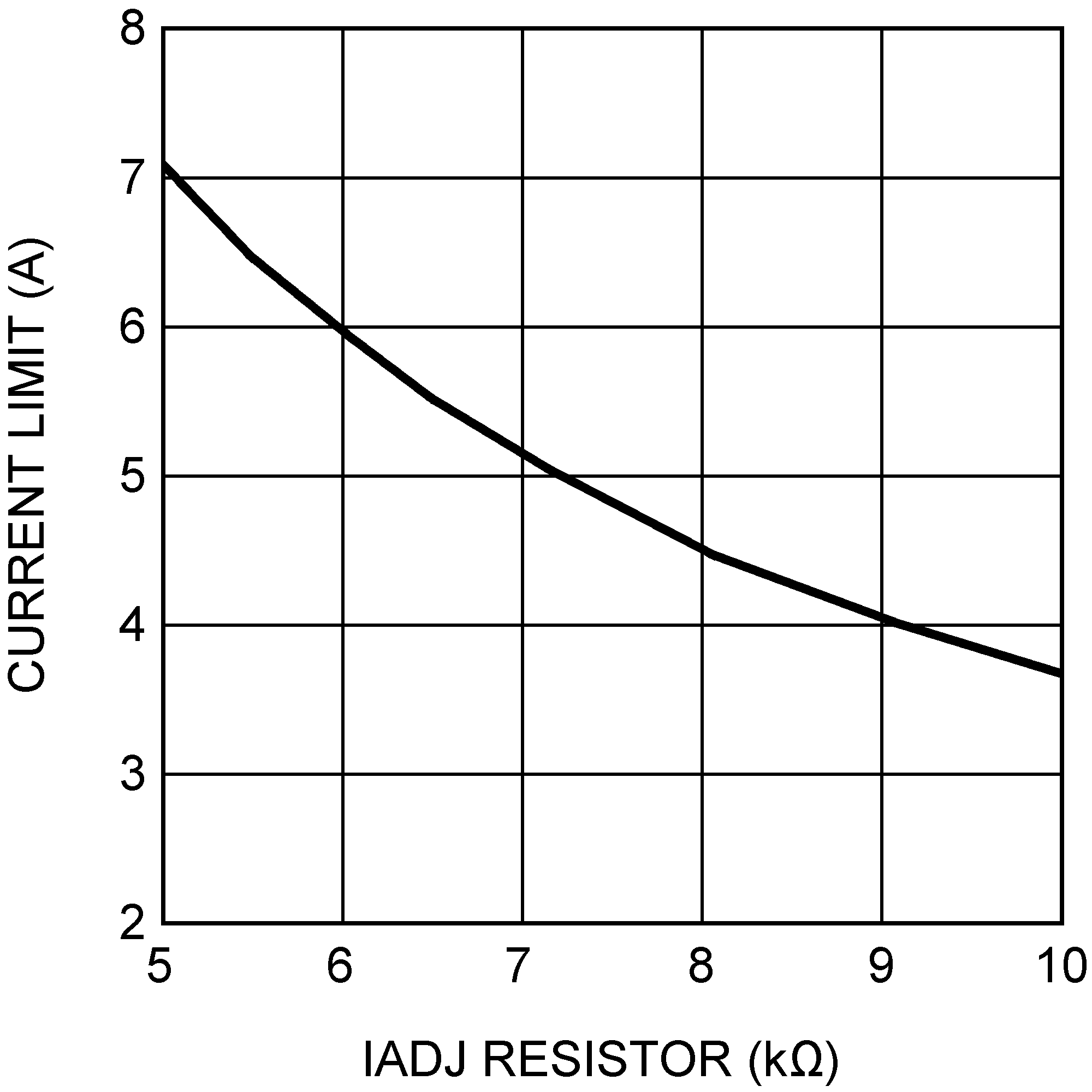
GUID-6FAF458E-0716-47FC-A73A-C016C9BDE504-low.pngFigure 6-9 Current Limit vs IADJ Resistor
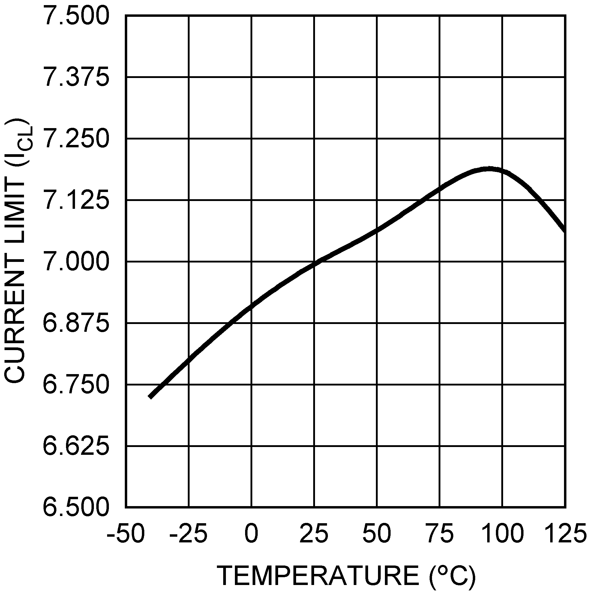
GUID-C2B11937-A62A-4A70-A6B7-34B869834602-low.pngFigure 6-2 Current Limit vs Temperature
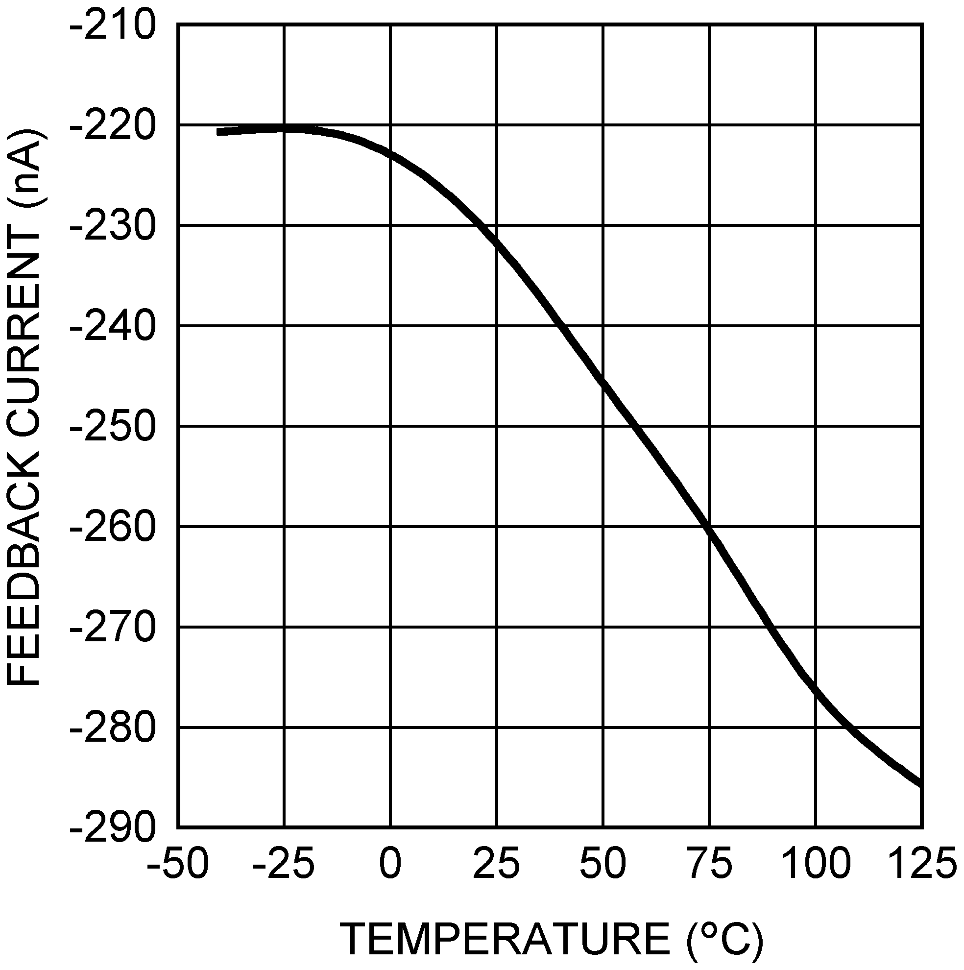
GUID-ACB7563A-A437-4600-BB1C-E597061BBB06-low.pngFigure 6-4 Feedback Bias Current vs Temperature
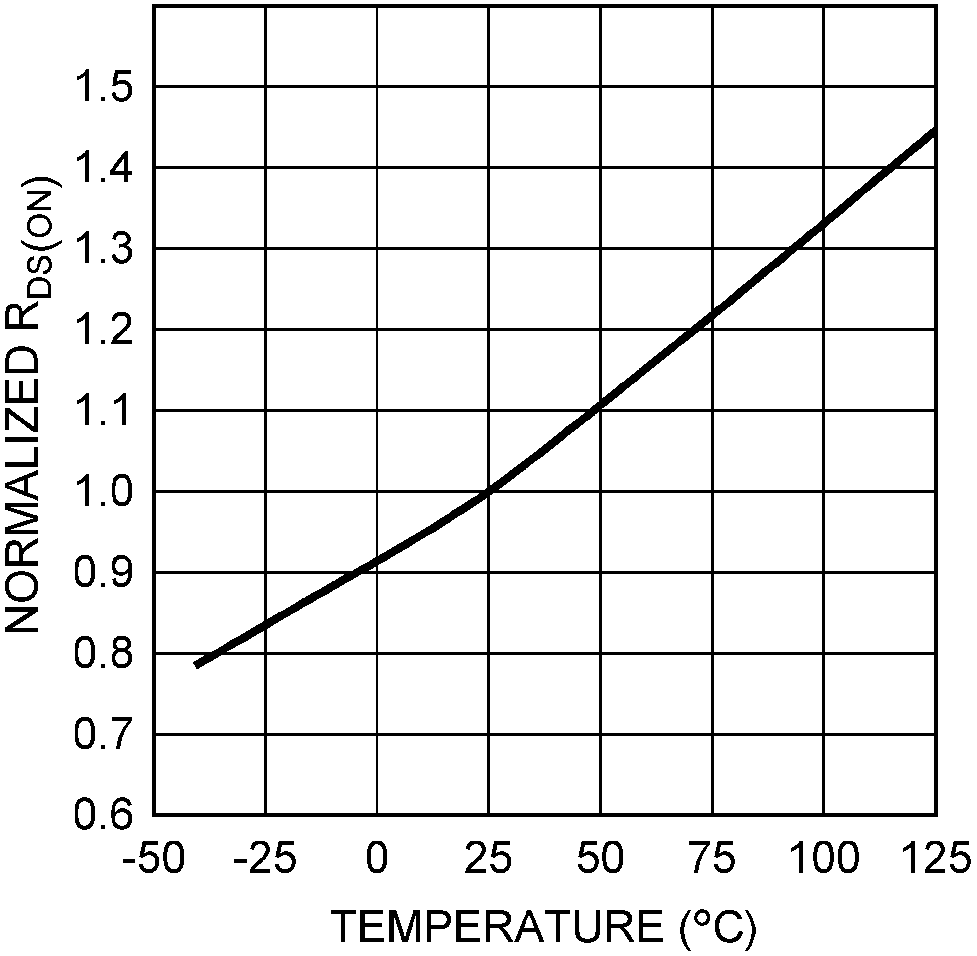
GUID-CF5E3E60-4661-4FD5-97EC-A45228C08281-low.pngFigure 6-6 Normalized RDS(ON) vs Temperature
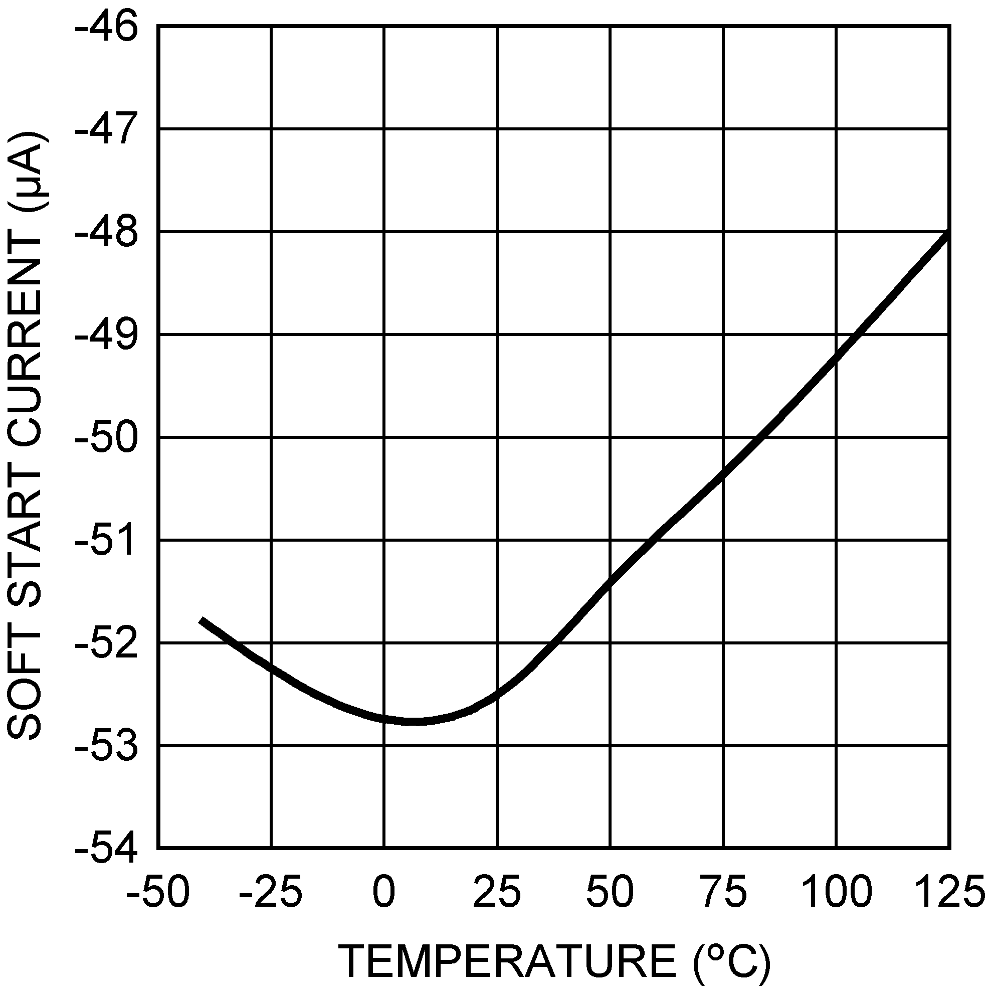
GUID-AE710A99-13EB-4135-8CEB-C787BE068957-low.pngFigure 6-8 Soft-Start Current vs Temperature