JAJSB11H April   2009  – November 2014 LM25011 , LM25011-Q1

PRODUCTION DATA.  

  1. 特長
  2. アプリケーション
  3. 概要
    1.     代表的なアプリケーション
  4. 改訂履歴
  5. Pin Configuration and Functions
    1.     Pin Functions
  6. Specifications
    1. 6.1 Absolute Maximum Ratings
    2. 6.2 Handling Ratings: LM25011
    3. 6.3 Handling Ratings: LM25011-Q1
    4. 6.4 Recommended Operating Conditions
    5. 6.5 Thermal Information
    6. 6.6 Electrical Characteristics
    7. 6.7 Typical Characteristics
  7. Detailed Description
    1. 7.1 Overview
    2. 7.2 Functional Block Diagram
    3. 7.3 Feature Description
      1. 7.3.1 Control Circuit Overview
      2. 7.3.2 On-Time Timer
      3. 7.3.3 Current Limit
      4. 7.3.4 Ripple Requirements
      5. 7.3.5 N-Channel Buck Switch and Driver
      6. 7.3.6 Soft-Start
      7. 7.3.7 Power Good Output (PGD)
      8. 7.3.8 Thermal Shutdown
    4. 7.4 Device Functional Modes
      1. 7.4.1 Shutdown Function
  8. Application and Implementation
    1. 8.1 Application Information
    2. 8.2 Typical Application
      1. 8.2.1 LM25011 Example Circuit
        1. 8.2.1.1 Design Requirements
        2. 8.2.1.2 Detailed Design Procedure
          1. 8.2.1.2.1 Custom Design with WEBENCH Tools
          2. 8.2.1.2.2 External Components
        3. 8.2.1.3 Application Curves
      2. 8.2.2 Output Ripple Control
        1. 8.2.2.1 Option A: Lowest Cost Configuration
        2. 8.2.2.2 Option B: Intermediate VOUT Ripple Configuration
        3. 8.2.2.3 Option C: Minimum VOUT Ripple Configuration
  9. Power Supply Recommendations
  10. 10Layout
    1. 10.1 Layout Guidelines
    2. 10.2 Layout Example
    3. 10.3 Power Dissipation
  11. 11デバイスおよびドキュメントのサポート
    1. 11.1 WEBENCHツールによるカスタム設計
    2. 11.2 ドキュメントの更新通知を受け取る方法
    3. 11.3 関連リンク
    4. 11.4 商標
    5. 11.5 静電気放電に関する注意事項
    6. 11.6 Glossary
  12. 12メカニカル、パッケージ、および注文情報

パッケージ・オプション

メカニカル・データ(パッケージ|ピン)
サーマルパッド・メカニカル・データ
発注情報

Typical Characteristics

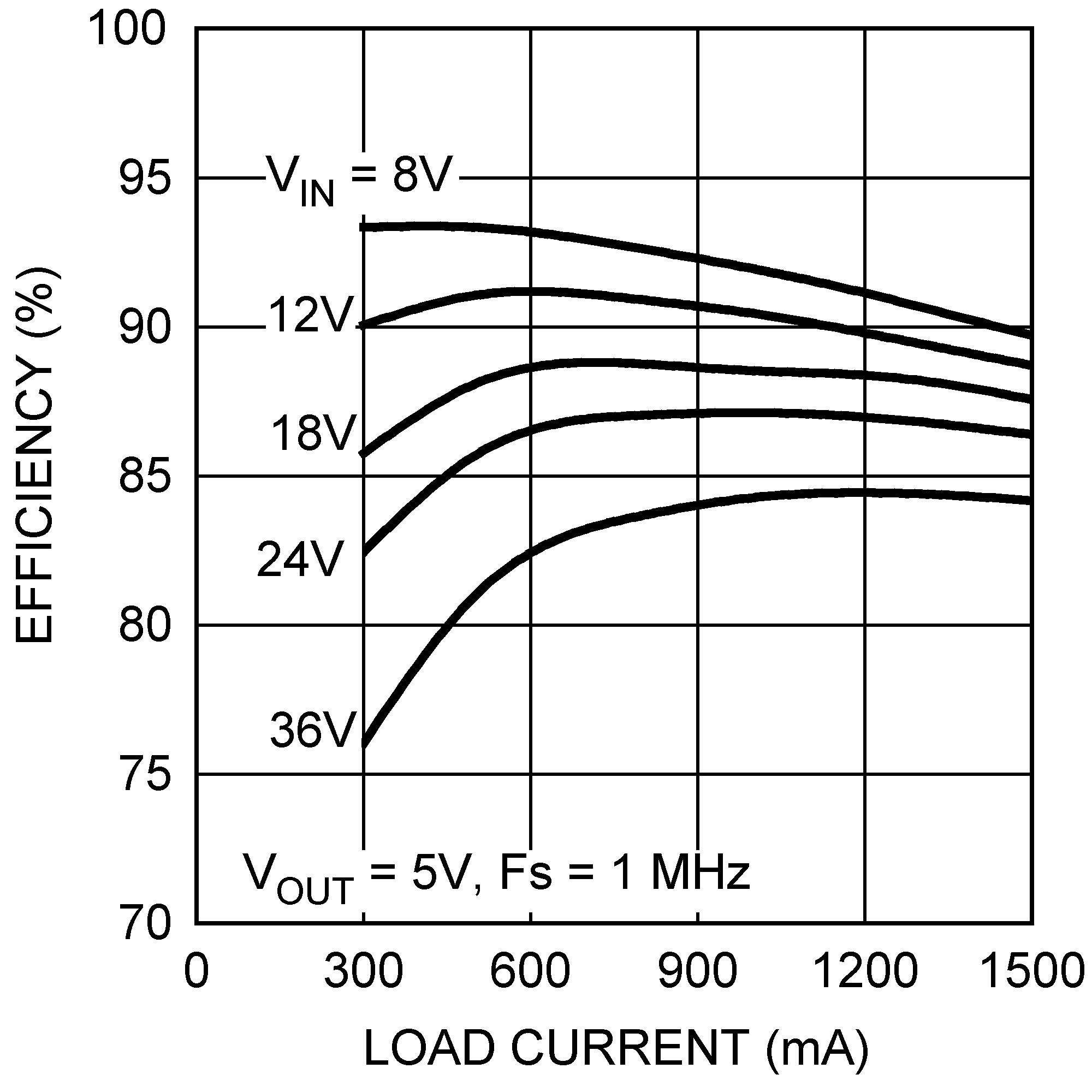
LM25011 LM25011-Q1 LM25011A LM25011A-Q1 30094603.pngFigure 1. Efficiency (Circuit of Figure 19)
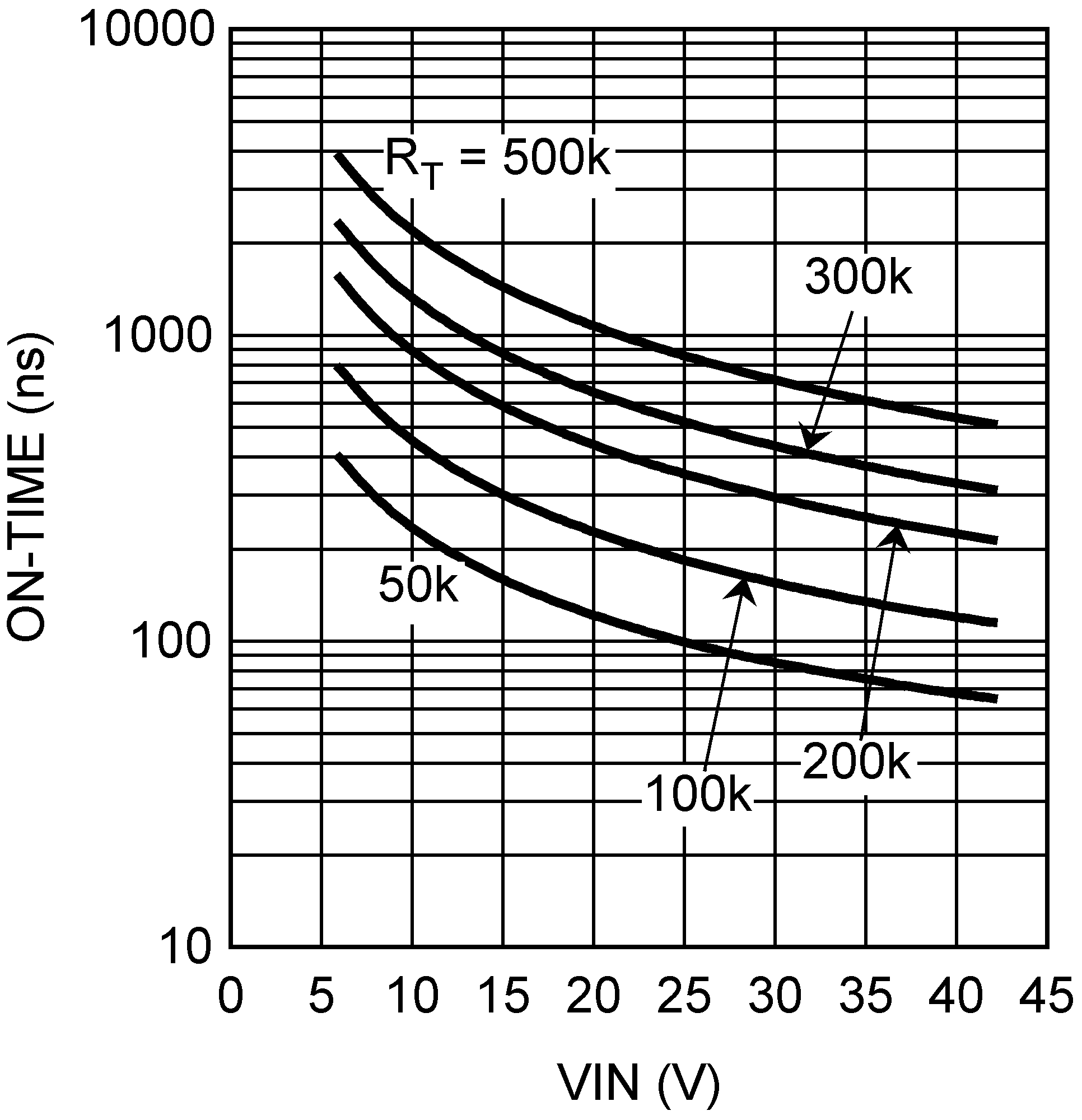
LM25011 LM25011-Q1 LM25011A LM25011A-Q1 30094605.pngFigure 3. On-Time vs VIN and RT
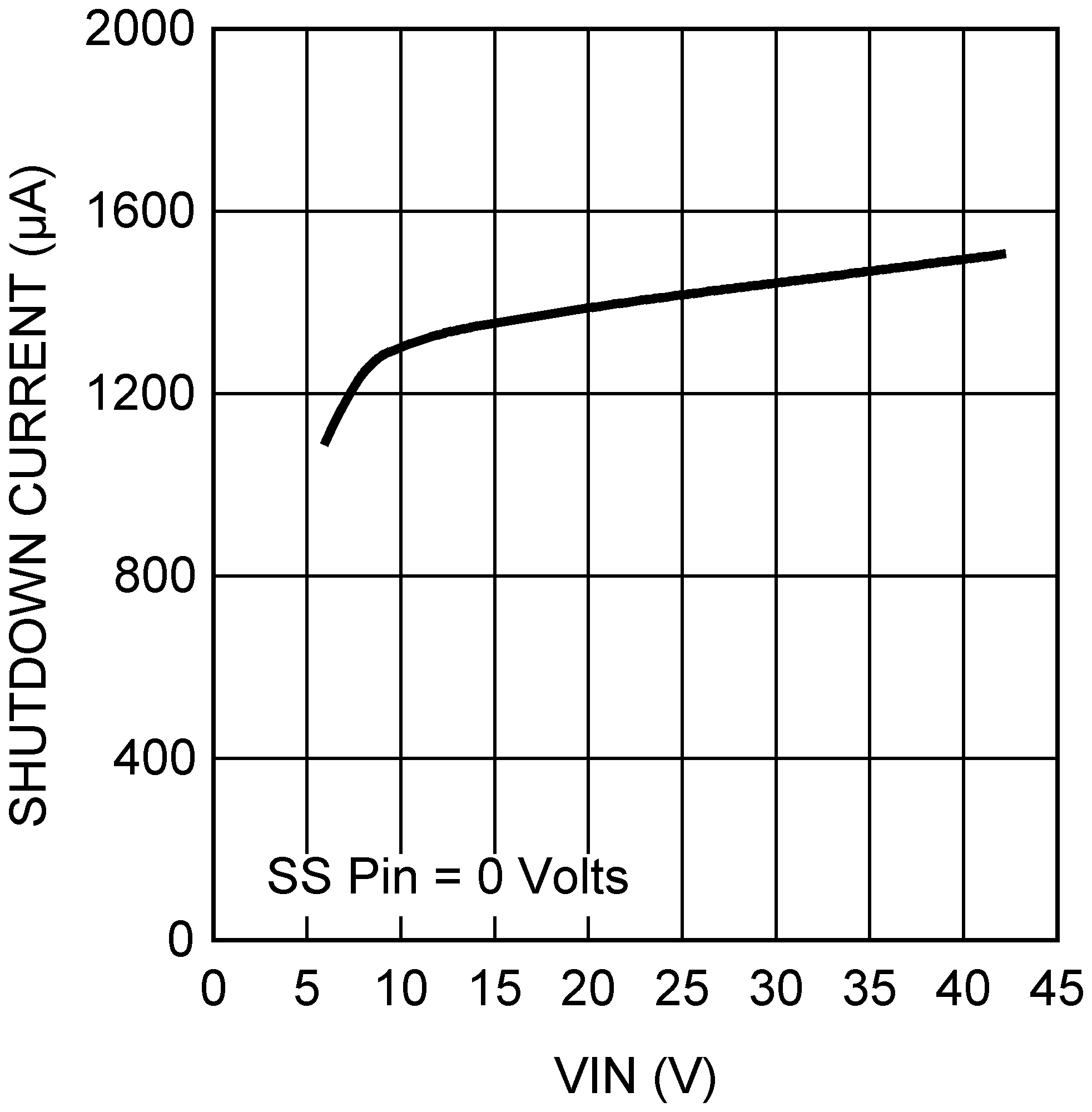
LM25011 LM25011-Q1 LM25011A LM25011A-Q1 30094607.pngFigure 5. Shutdown Current into VIN
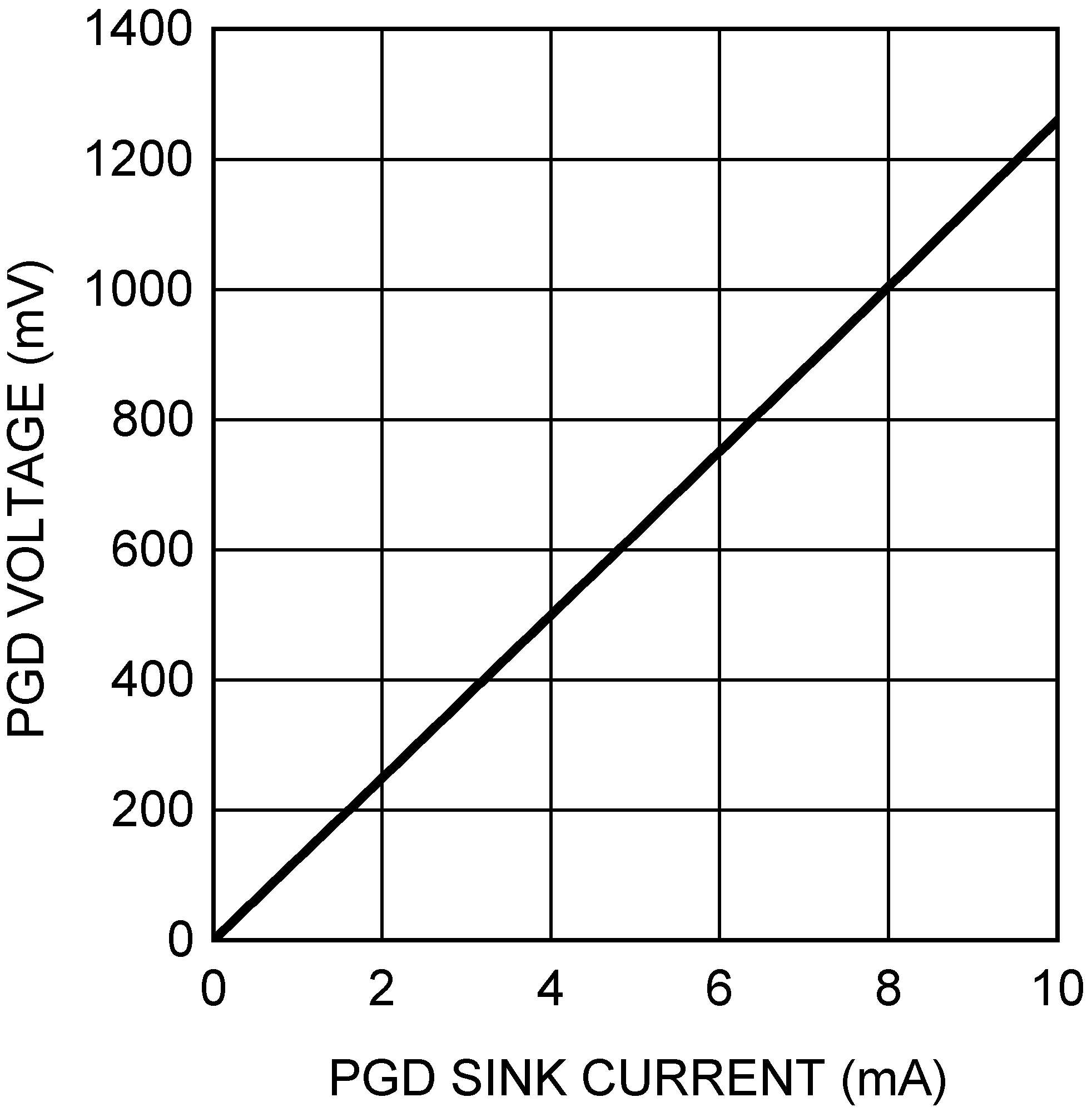
LM25011 LM25011-Q1 LM25011A LM25011A-Q1 30094609.pngFigure 7. PGD Low Voltage vs Sink Current
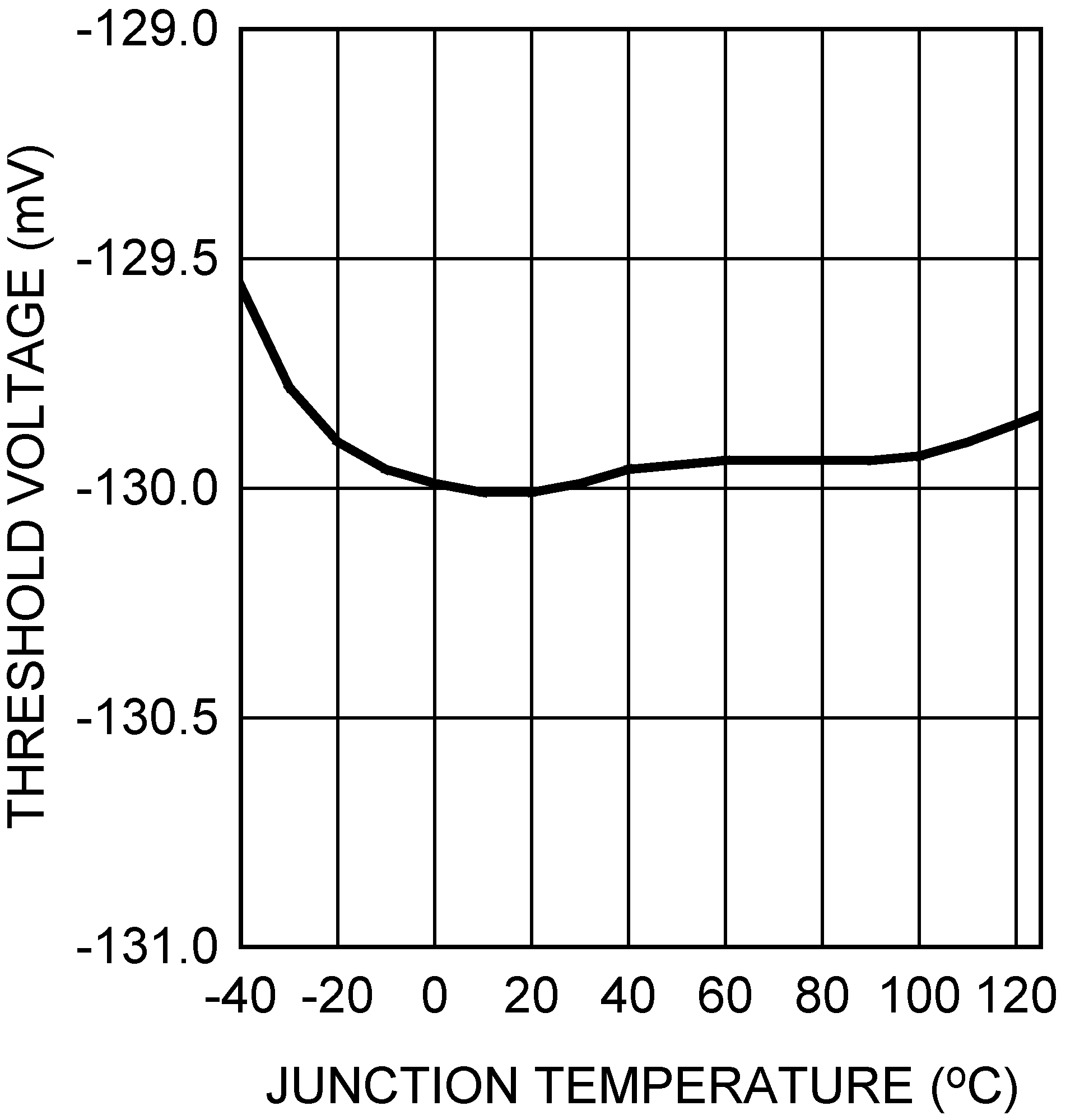
LM25011 LM25011-Q1 LM25011A LM25011A-Q1 30094611.pngFigure 9. Current Limit Threshold vs Temperature
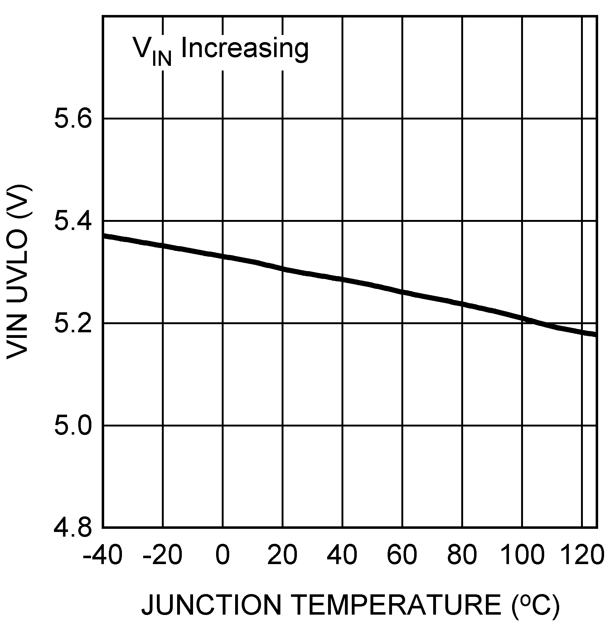
LM25011 LM25011-Q1 LM25011A LM25011A-Q1 30094613.pngFigure 11. VIN UVLO vs Temperature
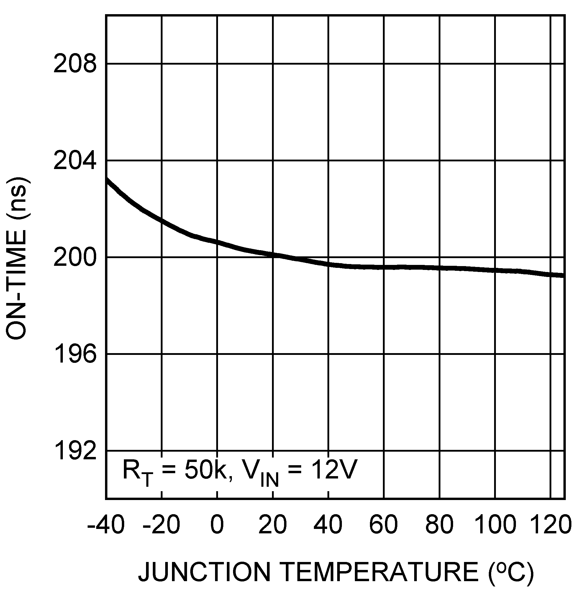
LM25011 LM25011-Q1 LM25011A LM25011A-Q1 30094615.pngFigure 13. On-Time vs Temperature
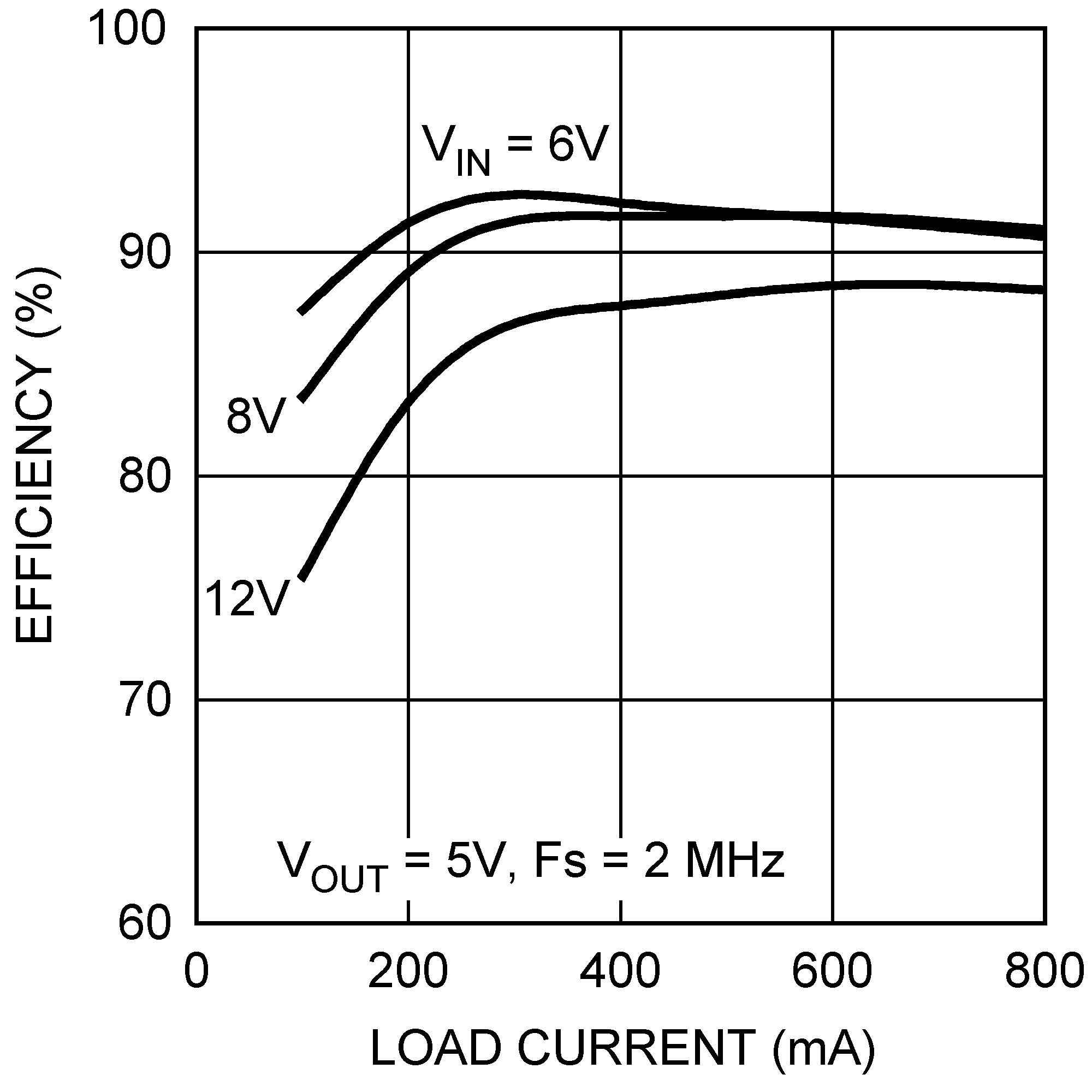
LM25011 LM25011-Q1 LM25011A LM25011A-Q1 30094604.pngFigure 2. Efficiency at 2 MHz
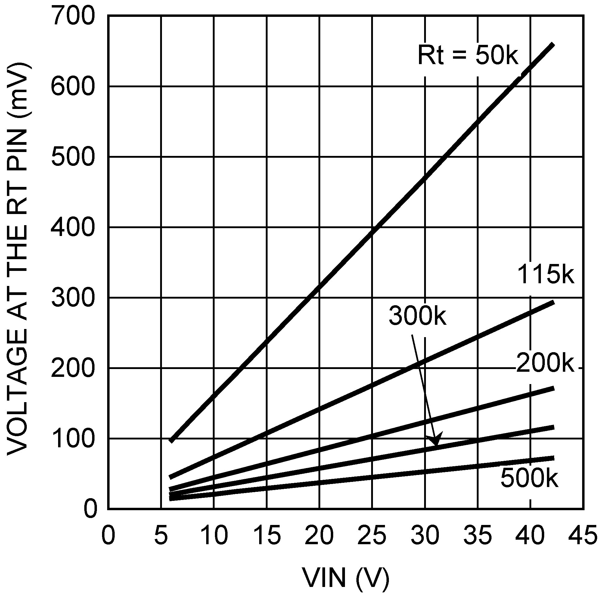
LM25011 LM25011-Q1 LM25011A LM25011A-Q1 30094606.pngFigure 4. Voltage at the RT Pin
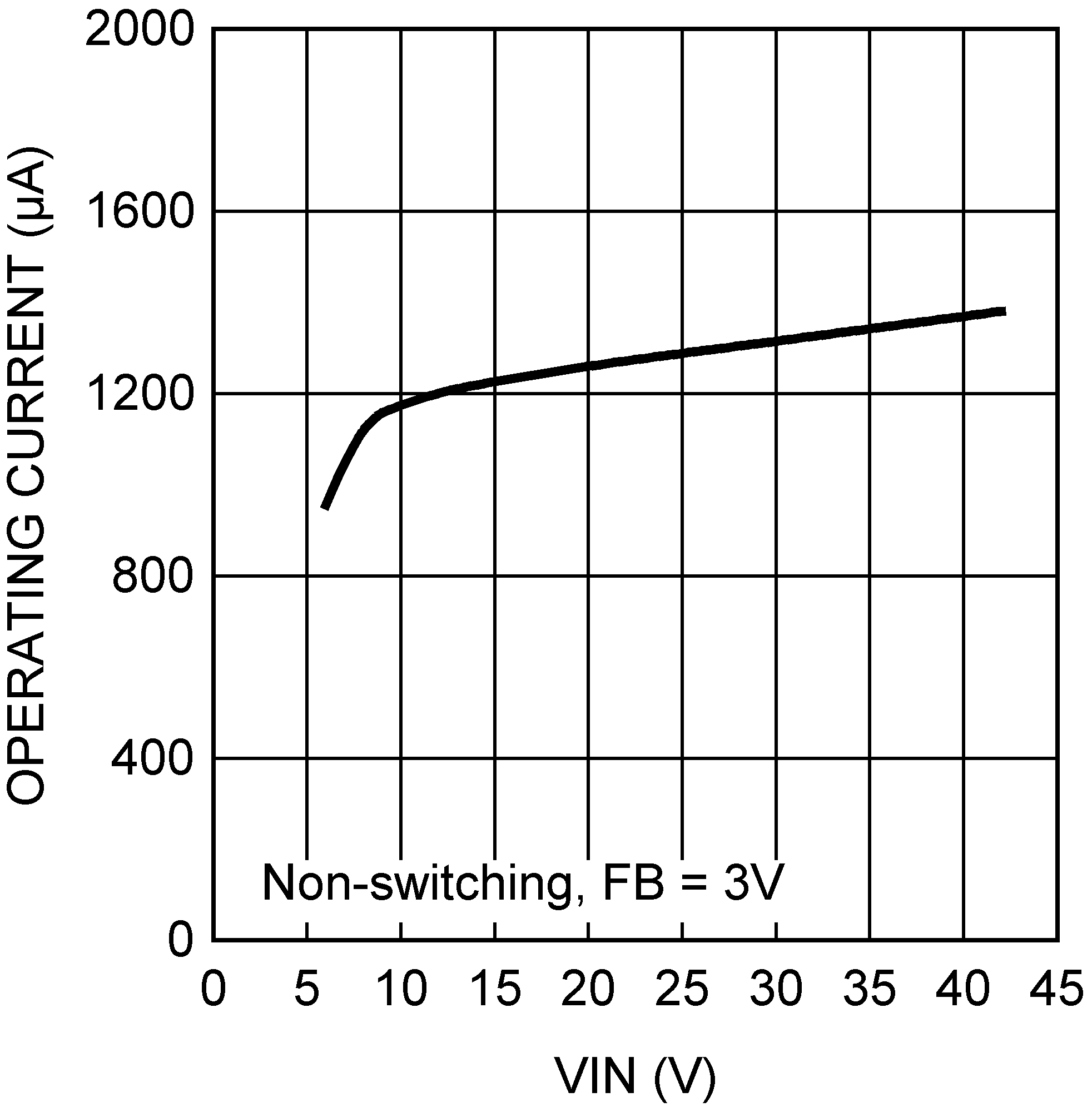
LM25011 LM25011-Q1 LM25011A LM25011A-Q1 30094608.pngFigure 6. Operating Current into VIN
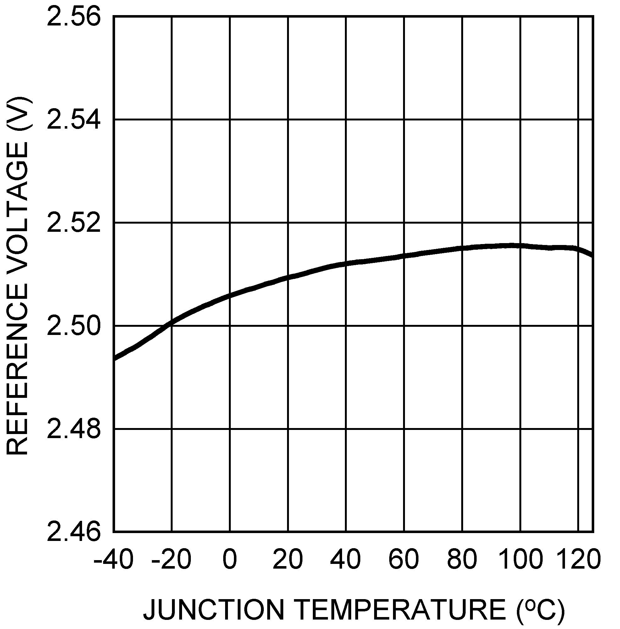
LM25011 LM25011-Q1 LM25011A LM25011A-Q1 30094610.pngFigure 8. Reference Voltage vs Temperature
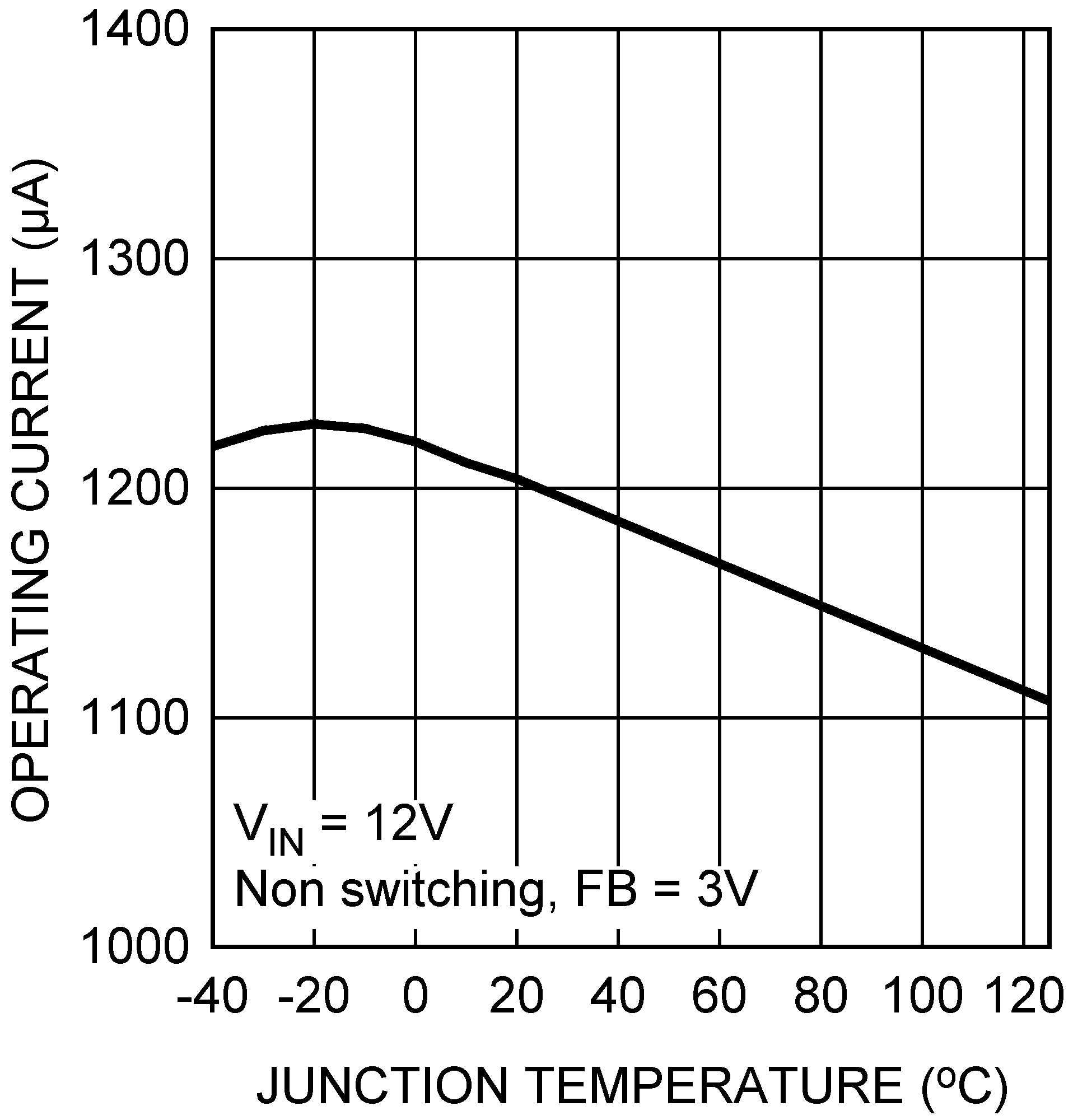
LM25011 LM25011-Q1 LM25011A LM25011A-Q1 30094612.pngFigure 10. Operating Current vs Temperature
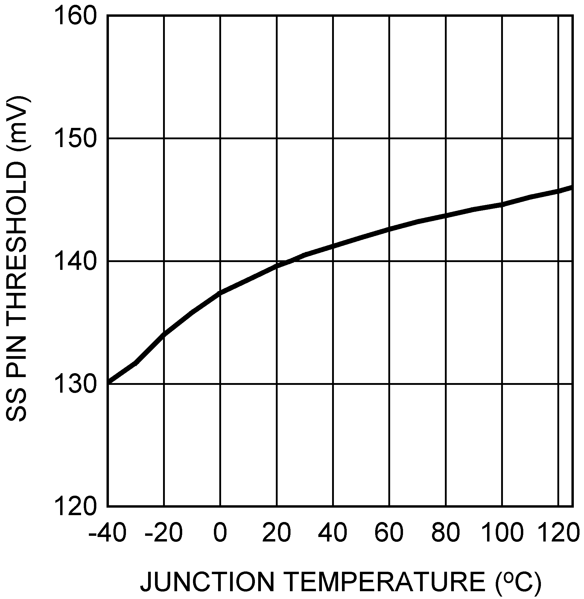
LM25011 LM25011-Q1 LM25011A LM25011A-Q1 30094614.pngFigure 12. SS Pin Shutdown Threshold vs Temperature
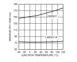
LM25011 LM25011-Q1 LM25011A LM25011A-Q1 30094651.gifFigure 14. Minimum Off-Time vs Temperature