JAJSCZ3A March 2017 – February 2018 LM25141-Q1
PRODUCTION DATA.
- 1 特長
- 2 アプリケーション
- 3 概要
- 4 改訂履歴
- 5 概要(続き)
- 6 Pin Configuration and Functions
- 7 Specifications
-
8 Detailed Description
- 8.1 Overview
- 8.2 Functional Block Diagram
- 8.3
Feature Description
- 8.3.1 High Voltage Start-Up Regulator
- 8.3.2 VCC Regulator
- 8.3.3 Oscillator
- 8.3.4 Synchronization
- 8.3.5 Frequency Dithering (Spread Spectrum)
- 8.3.6 Enable
- 8.3.7 Power Good
- 8.3.8 Output Voltage
- 8.3.9 Current Sense
- 8.3.10 DCR Current Sensing
- 8.3.11 Error Amplifier and PWM Comparator
- 8.3.12 Slope Compensation
- 8.3.13 Hiccup Mode Current Limiting
- 8.3.14 Standby Mode
- 8.3.15 Soft Start
- 8.3.16 Diode Emulation
- 8.3.17 High- and Low-Side Drivers
-
9 Application and Implementation
- 9.1 Application Information
- 9.2 Typical Application
- 10Power Supply Recommendations
- 11Layout
- 12デバイスおよびドキュメントのサポート
- 13メカニカル、パッケージ、および注文情報
パッケージ・オプション
メカニカル・データ(パッケージ|ピン)
- RGE|24
サーマルパッド・メカニカル・データ
- RGE|24
発注情報
8.3.9 Current Sense
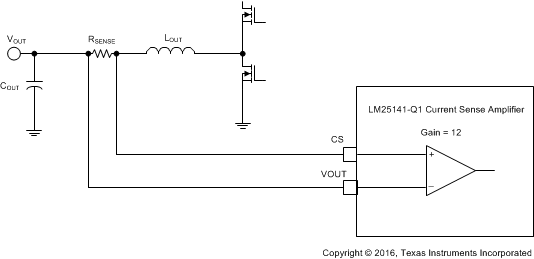
There are two methods to sense the inductor current of the buck converter. The first is using current sense resistor in series with the inductor and the second is to use the DC resistance of the inductor (DCR sensing). Figure 24 illustrates inductor current sensing using a current sense resistor. This configuration continuously monitors the inductor current providing accurate current-limit protection. For the best current-sense accuracy and over current protection, use a low inductance ±1% tolerance current-sense resistor between the inductor and output, with a Kelvin connection to the LM25141-Q1 sense amplifier.
If the peak differential current signal sensed from CS to VOUT exceeds 75 mV, the current limit comparator immediately terminates the HO output for cycle-by-cycle current limiting.

where
- V(CS) = 75 mV
IOUT(MAX) is the overcurrent set-point which is set higher than the maximum load current to avoid tripping the overcurrent comparator during load transients. ΔI is the peak-peak inductor ripple current.
 Figure 24. Current Sense