JAJS772E June 1999 – July 2018 LM2574 , LM2574HV
PRODUCTION DATA.
- 1 特長
- 2 アプリケーション
- 3 概要
- 4 改訂履歴
- 5 Pin Configuration and Functions
-
6 Specifications
- 6.1 Absolute Maximum Ratings
- 6.2 ESD Ratings
- 6.3 Recommended Operating Conditions
- 6.4 Thermal Information
- 6.5 Electrical Characteristics for All Output Voltage Versions
- 6.6 Electrical Characteristics – 3.3-V Version
- 6.7 Electrical Characteristics – 5-V Version
- 6.8 Electrical Characteristics – 12-V Version
- 6.9 Electrical Characteristics – 15-V Version
- 6.10 Electrical Characteristics – Adjustable Version
- 6.11 Typical Characteristics
- 7 Detailed Description
-
8 Application and Implementation
- 8.1 Application Information
- 8.2 Typical Applications
- 9 Power Supply Recommendations
- 10Layout
-
11デバイスおよびドキュメントのサポート
- 11.1
デバイス・サポート
- 11.1.1 デベロッパー・ネットワークの製品に関する免責事項
- 11.1.2 WEBENCH®ツールによるカスタム設計
- 11.1.3
デバイスの項目表記
- 11.1.3.1 降圧レギュレータ
- 11.1.3.2 昇降圧レギュレータ
- 11.1.3.3 デューティ・サイクル(D)
- 11.1.3.4 キャッチ・ダイオードまたは電流ステアリング・ダイオード
- 11.1.3.5 コンデンサの等価直列抵抗(ESR)
- 11.1.3.6 等価直列インダクタンス(ESL)
- 11.1.3.7 出力リップル電圧
- 11.1.3.8 コンデンサのリップル電流
- 11.1.3.9 スタンバイ時静止電流(ISTBY)
- 11.1.3.10 インダクタのリップル電流(ΔIIND)
- 11.1.3.11 連続/不連続モードの動作
- 11.1.3.12 インダクタの飽和
- 11.1.3.13 動作電圧のマイクロ秒定数(E・Top)
- 11.2 ドキュメントのサポート
- 11.3 ドキュメントの更新通知を受け取る方法
- 11.4 コミュニティ・リソース
- 11.5 商標
- 11.6 静電気放電に関する注意事項
- 11.7 Glossary
- 11.1
デバイス・サポート
- 12メカニカル、パッケージ、および注文情報
パッケージ・オプション
メカニカル・データ(パッケージ|ピン)
サーマルパッド・メカニカル・データ
発注情報
8.1.3 Inductor Ripple Current
When the switcher is operating in the continuous mode, the inductor current waveform ranges from a triangular to a sawtooth type of waveform (depending on the input voltage). For a given input voltage and output voltage, the peak-to-peak amplitude of this inductor current waveform remains constant. As the load current rises or falls, the entire sawtooth current waveform also rises or falls. The average DC value of this waveform is equal to the DC load current (in the buck regulator configuration).
If the load current drops to a low enough level, the bottom of the sawtooth current waveform reaches zero, and the switcher changes to a discontinuous mode of operation. This is a perfectly acceptable mode of operation. Any buck switching regulator (no matter how large the inductor value is) is forced to run discontinuous if the load current is light enough.
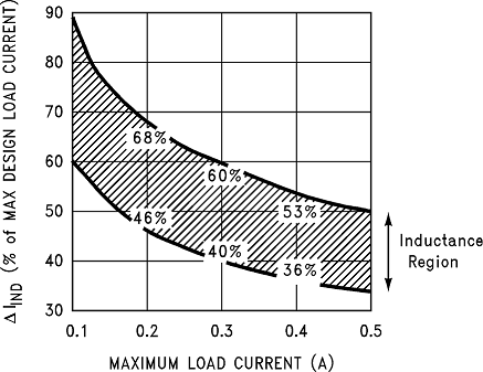
The curve shown in Figure 19 illustrates how the peak-to-peak inductor ripple current (ΔIIND) is allowed to change as different maximum load currents are selected, and also how it changes as the operating point varies from the upper border to the lower border within an inductance region (see Inductor Selection).
 Figure 19. Inductor Ripple Current (ΔiIND) Range
 Consider the following example:
VOUT = 5 V at 0.4 A
VIN = 10-V minimum up to 20-V maximum
The selection guide in Figure 24 shows that for a 0.4-A load current, and an input voltage range between 10 V and 20 V, the inductance region selected by the guide is 330 μH. This value of inductance allows a peak-to-peak inductor ripple current (ΔIIND) to flow that is a percentage of the maximum load current. For this inductor value, the ΔIIND also varies depending on the input voltage. As the input voltage increases to 20 V, it approaches the upper border of the inductance region, and the inductor ripple current increases. Referring to the curve in Figure 19, it can be seen that at the 0.4-A load current level, and operating near the upper border of the 330-μH inductance region, the ΔIIND is 53% of 0.4 A, or 212 mAp-p.
This ΔIIND is important because from this number the peak inductor current rating can be determined, the minimum load current required before the circuit goes to discontinuous operation, and also, knowing the ESR of the output capacitor, the output ripple voltage can be calculated, or conversely, measuring the output ripple voltage and knowing the ΔIIND, the ESR can be calculated.
From the previous example, the peak-to-peak inductor ripple current (ΔIIND) = 212 mAp-p. When the ΔIND value is known, the following three formulas can be used to calculate additional information about the switching regulator circuit:
- Peak inductor or peak switch current in Equation 3.
- Minimum load current before the circuit becomes discontinuous in Equation 4.
- Output ripple voltage = (ΔIIND) × (ESR of COUT)


The selection guide chooses inductor values suitable for continuous mode operation, but if the inductor value chosen is prohibitively high, the designer should investigate the possibility of discontinuous operation.
Inductors are available in different styles such as pot core, toroid, E-frame, bobbin core, and so forth, as well as different core materials, such as ferrites and powdered iron. The least expensive, the bobbin core type, consists of wire wrapped on a ferrite rod core. This type of construction makes for an inexpensive inductor, but because the magnetic flux is not completely contained within the core, it generates more electro-magnetic interference (EMI). This EMl can cause problems in sensitive circuits, or can give incorrect scope readings because of induced voltages in the scope probe.
The inductors listed in the selection chart include powdered iron toroid for Pulse Engineering, and ferrite bobbin core for Renco.
An inductor must not be operated beyond its maximum rated current because it may saturate. When an inductor begins to saturate, the inductance decreases rapidly and the inductor begins to look mainly resistive (the DC resistance of the winding). This can cause the inductor current to rise very rapidly and affects the energy storage capabilities of the inductor and could cause inductor overheating. Different inductor types have different saturation characteristics, and consider this when selecting an inductor. The inductor manufacturers' data sheets include current and energy limits to avoid inductor saturation.