JAJS782G june   1999  – march 2023 LM2576 , LM2576HV

PRODUCTION DATA  

  1. 特長
  2. アプリケーション
  3. 概要
  4. Revision History
  5. Pin Configuration and Functions
  6. Specifications
    1. 6.1  Absolute Maximum Ratings
    2. 6.2  ESD Ratings
    3. 6.3  Recommended Operating Conditions
    4. 6.4  Thermal Information
    5. 6.5  Electrical Characteristics: 3.3 V
    6. 6.6  Electrical Characteristics: 5 V
    7. 6.7  Electrical Characteristics: 12 V
    8. 6.8  Electrical Characteristics: 15 V
    9. 6.9  Electrical Characteristics: Adjustable Output Voltage
    10. 6.10 Electrical Characteristics: All Output Voltage Versions
    11. 6.11 Typical Characteristics
  7. Detailed Description
    1. 7.1 Overview
    2. 7.2 Functional Block Diagram
    3. 7.3 Feature Description
      1. 7.3.1 Undervoltage Lockout
      2. 7.3.2 Delayed Start-Up
      3. 7.3.3 Adjustable Output, Low-Ripple Power Supply
    4. 7.4 Device Functional Modes
      1. 7.4.1 Shutdown Mode
      2. 7.4.2 Active Mode
      3. 7.4.3 Current Limit
  8. Application and Implementation
    1. 8.1 Application Information
      1. 8.1.1  Input Capacitor (CIN)
      2. 8.1.2  Inductor Selection
      3. 8.1.3  Inductor Ripple Current
      4. 8.1.4  Output Capacitor
      5. 8.1.5  Catch Diode
      6. 8.1.6  Output Voltage Ripple and Transients
      7. 8.1.7  Feedback Connection
      8. 8.1.8  ON /OFF INPUT
      9. 8.1.9  Inverting Regulator
      10. 8.1.10 Negative Boost Regulator
    2. 8.2 Typical Applications
      1. 8.2.1 Fixed Output Voltage Version
        1. 8.2.1.1 Design Requirements
        2. 8.2.1.2 Detailed Design Procedure
          1. 8.2.1.2.1 Custom Design with WEBENCH® Tools
          2. 8.2.1.2.2 Inductor Selection (L1)
          3. 8.2.1.2.3 Output Capacitor Selection (COUT)
          4. 8.2.1.2.4 Catch Diode Selection (D1)
          5. 8.2.1.2.5 Input Capacitor (CIN)
        3. 8.2.1.3 Application Curves
      2. 8.2.2 Adjusted Output Voltage Version
        1. 8.2.2.1 Design Requirements
        2. 8.2.2.2 Detailed Design Procedure
          1. 8.2.2.2.1 Programming Output Voltage
          2. 8.2.2.2.2 Inductor Selection (L1)
          3. 8.2.2.2.3 Output Capacitor Selection (COUT)
          4. 8.2.2.2.4 Catch Diode Selection (D1)
          5. 8.2.2.2.5 Input Capacitor (CIN)
    3. 8.3 Power Supply Recommendations
    4. 8.4 Layout
      1. 8.4.1 Layout Guidelines
      2. 8.4.2 Layout Example
      3. 8.4.3 Grounding
      4. 8.4.4 Heat Sink and Thermal Considerations
  9. Device and Documentation Support
    1. 9.1 Device Support
      1. 9.1.1 Device Nomenclature
        1. 9.1.1.1 Definition of Terms
      2. 9.1.2 Development Support
        1. 9.1.2.1 Custom Design with WEBENCH® Tools
    2. 9.2 Documentation Support
      1. 9.2.1 Related Documentation
    3. 9.3 サポート・リソース
    4. 9.4 ドキュメントの更新通知を受け取る方法
    5. 9.5 Trademarks
    6. 9.6 静電気放電に関する注意事項
    7. 9.7 用語集
  10. 10Mechanical, Packaging, and Orderable Information

パッケージ・オプション

デバイスごとのパッケージ図は、PDF版データシートをご参照ください。

メカニカル・データ(パッケージ|ピン)
  • NDH|5
  • NEB|5
  • KTT|5
  • KC|5
サーマルパッド・メカニカル・データ
発注情報

Negative Boost Regulator

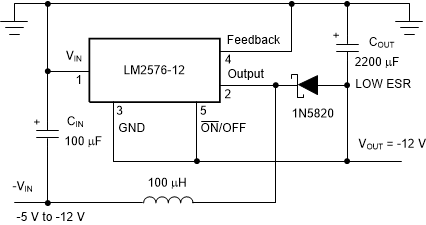
Another variation on the buck-boost topology is the negative boost configuration. The circuit in Figure 8-2 accepts an input voltage ranging from −5 V to −12 V and provides a regulated −12-V output. Input voltages greater than −12 V causes the output to rise above −12 V, but does not damage the regulator.
GUID-EE44F562-31BB-497B-8FA6-DFBDA882F3D4-low.gif
Typical Load Current 400 mA for VIN = −5.2 V 750 mA for VIN = −7 V Heat sink can be required.
Figure 8-2 Negative Boost

Because of the boosting function of this type of regulator, the switch current is relatively high, especially at low input voltages. Output load current limitations are a result of the maximum current rating of the switch. Also, boost regulators can not provide current-limiting load protection in the event of a shorted load, so some other means (such as a fuse) can be necessary.