JAJS843E April   1998  – June 2019 LM2588

PRODUCTION DATA.  

  1. 特長
  2. 代表的なアプリケーション
  3. 概要
    1.     Device Images
      1.      フライバック・レギュレータ
  4. 改訂履歴
  5. 概要(続き)
  6. Pin Configurations
  7. Specifications
    1. 7.1 Absolute Maximum Ratings
    2. 7.2 ESD Ratings
    3. 7.3 Recommended Operating Ratings
    4. 7.4 Electrical Characteristics: 3.3 V
    5. 7.5 Electrical Characteristics: 5 V
    6. 7.6 Electrical Characteristics: 12 V
    7. 7.7 Electrical Characteristics: Adjustable
    8. 7.8 Electrical Characteristics: All Output Voltage Versions
    9. 7.9 Typical Characteristics
  8. Detailed Description
    1. 8.1 Overview
    2. 8.2 Functional Block Diagram
    3. 8.3 Feature Description
      1. 8.3.1 Flyback Regulator Operation
      2. 8.3.2 Step-Up (Boost) Regulator Operation
      3. 8.3.3 Shutdown Control
      4. 8.3.4 Frequency Adjustment
      5. 8.3.5 Frequency Synchronization
      6. 8.3.6 Programming Output Voltage (Selecting R1 And R2)
      7. 8.3.7 Short-Circuit Condition
  9. Application and Implementation
    1. 9.1 Application Information
    2. 9.2 Typical Applications
      1. 9.2.1 Typical Flyback Regulator Applications
        1. 9.2.1.1 Design Requirements
          1. 9.2.1.1.1 Transformer Selection (T)
          2. 9.2.1.1.2 Transformer Footprints
        2. 9.2.1.2 Detailed Design Procedure
          1. 9.2.1.2.1 Custom Design With WEBENCH® Tools
          2. 9.2.1.2.2 Flyback Regulator Input Capacitors
          3. 9.2.1.2.3 Switch Voltage Limits
          4. 9.2.1.2.4 Output Voltage Limitations
          5. 9.2.1.2.5 Noisy Input Line Condition
          6. 9.2.1.2.6 Stability
      2. 9.2.2 Typical Boost Regulator Applications
        1. 9.2.2.1 Design Requirements
        2. 9.2.2.2 Detailed Design Procedure
    3. 9.3 System Examples
      1. 9.3.1 Test Circuits
  10. 10Layout
    1. 10.1 Layout Guidelines
    2. 10.2 Layout Example
    3. 10.3 Heat Sink/Thermal Considerations
  11. 11デバイスおよびドキュメントのサポート
    1. 11.1 デバイス・サポート
      1. 11.1.1 デベロッパー・ネットワークの製品に関する免責事項
      2. 11.1.2 開発サポート
        1. 11.1.2.1 WEBENCH®ツールによるカスタム設計
    2. 11.2 ドキュメントの更新通知を受け取る方法
    3. 11.3 コミュニティ・リソース
    4. 11.4 商標
    5. 11.5 静電気放電に関する注意事項
    6. 11.6 Glossary
  12. 12メカニカル、パッケージ、および注文情報

パッケージ・オプション

メカニカル・データ(パッケージ|ピン)
サーマルパッド・メカニカル・データ
発注情報

Flyback Regulator Operation

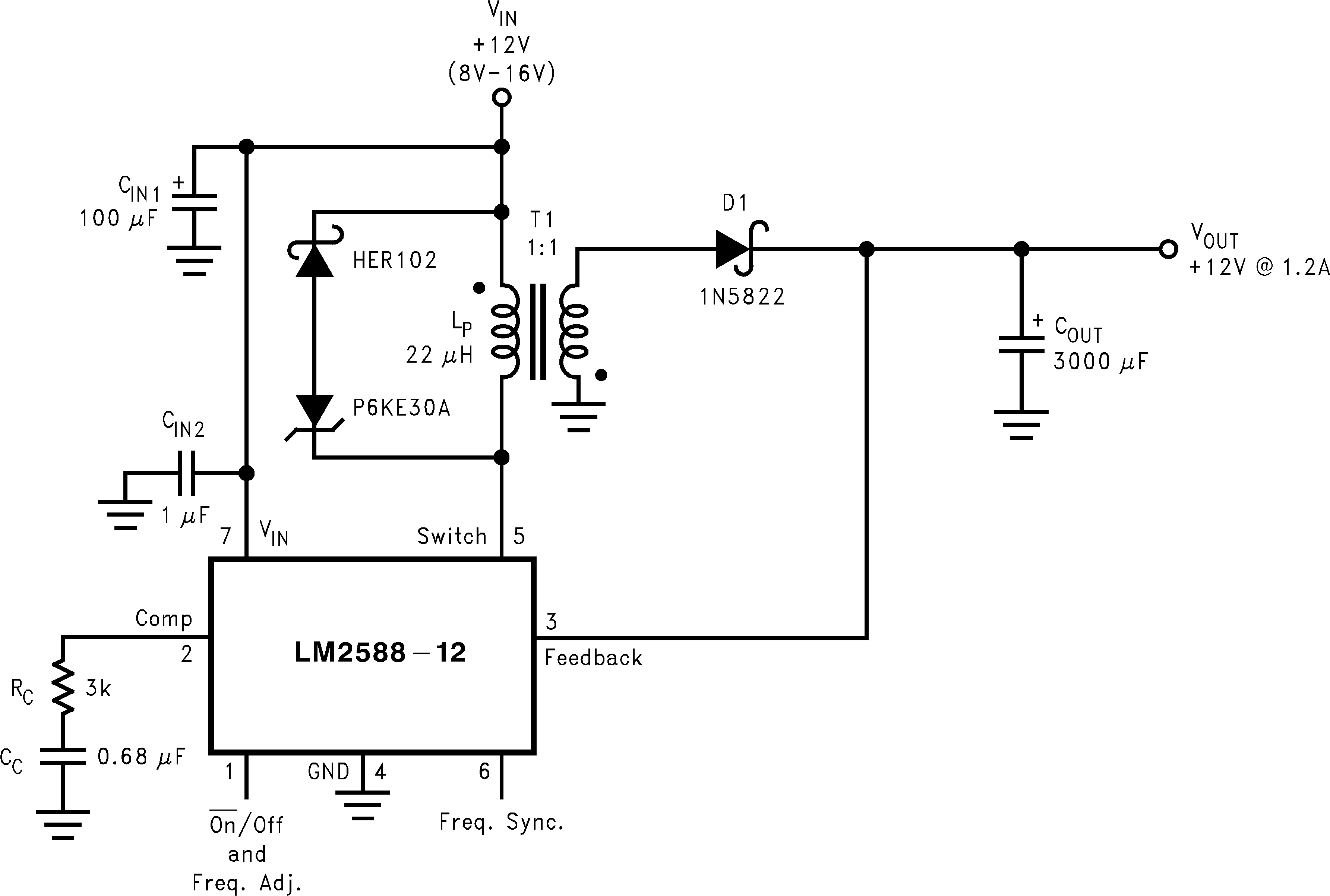
The operation of a flyback regulator is as follows (refer to Figure 16): when the switch is on, current flows through the primary winding of the transformer, T1, storing energy in the magnetic field of the transformer. Note that the primary and secondary windings are out of phase, so no current flows through the secondary when current flows through the primary. When the switch turns off, the magnetic field collapses, reversing the voltage polarity of the primary and secondary windings. Now rectifier D1 is forward biased and current flows through it, releasing the energy stored in the transformer. This produces voltage at the output.

The output voltage is controlled by modulating the peak switch current. This is done by feeding back a portion of the output voltage to the error amp, which amplifies the difference between the feedback voltage and a 1.23-V reference. The error amp output voltage is compared to a ramp voltage proportional to the switch current (in other words, inductor current during the switch on-time). The comparator terminates the switch on time when the two voltages are equal, thereby controlling the peak switch current to maintain a constant output voltage.
LM2588 01242024.png
As shown in Figure 16, the LM2588 can be used as a flyback regulator by using a minimum number of external components. The switching waveforms of this regulator are shown in Figure 18. Typical characteristics observed during the operation of this circuit are shown in Figure 19.
Figure 16. 12-V Flyback Regulator Design Example