SNVS075E May 2001 – May 2016 LM2592HV
PRODUCTION DATA.
- 1 Features
- 2 Applications
- 3 Description
- 4 Revision History
- 5 Description (continued)
- 6 Pin Configuration and Functions
-
7 Specifications
- 7.1 Absolute Maximum Ratings
- 7.2 ESD Ratings
- 7.3 Recommended Operating Conditions
- 7.4 Thermal Information
- 7.5 Electrical Characteristics LM2592HV-3.3
- 7.6 Electrical Characteristics LM2592HV-5.0
- 7.7 Electrical Characteristics LM2592HV-ADJ
- 7.8 Electrical Characteristics All Output Voltage Versions
- 7.9 Typical Characteristics
- 8 Parameter Measurement Information
- 9 Detailed Description
- 10Application and Implementation
- 11Power Supply Recommendations
- 12Layout
- 13Device and Documentation Support
- 14Mechanical, Packaging, and Orderable Information
パッケージ・オプション
メカニカル・データ(パッケージ|ピン)
サーマルパッド・メカニカル・データ
発注情報
9 Detailed Description
9.1 Overview
The LM2592HV SIMPLE SWITCHER® regulator is an easy-to-use, nonsynchronous, step-down DC-DC converter with a wide input voltage range up to 60 V. The regulator is capable of delivering up to 2-A DC load current with excellent line and load regulation. These devices are available in fixed output voltages of 3.3 V, 5 V, and an adjustable output version. The family requires few external components, and the pin arrangement was designed for simple, optimum PCB layout.
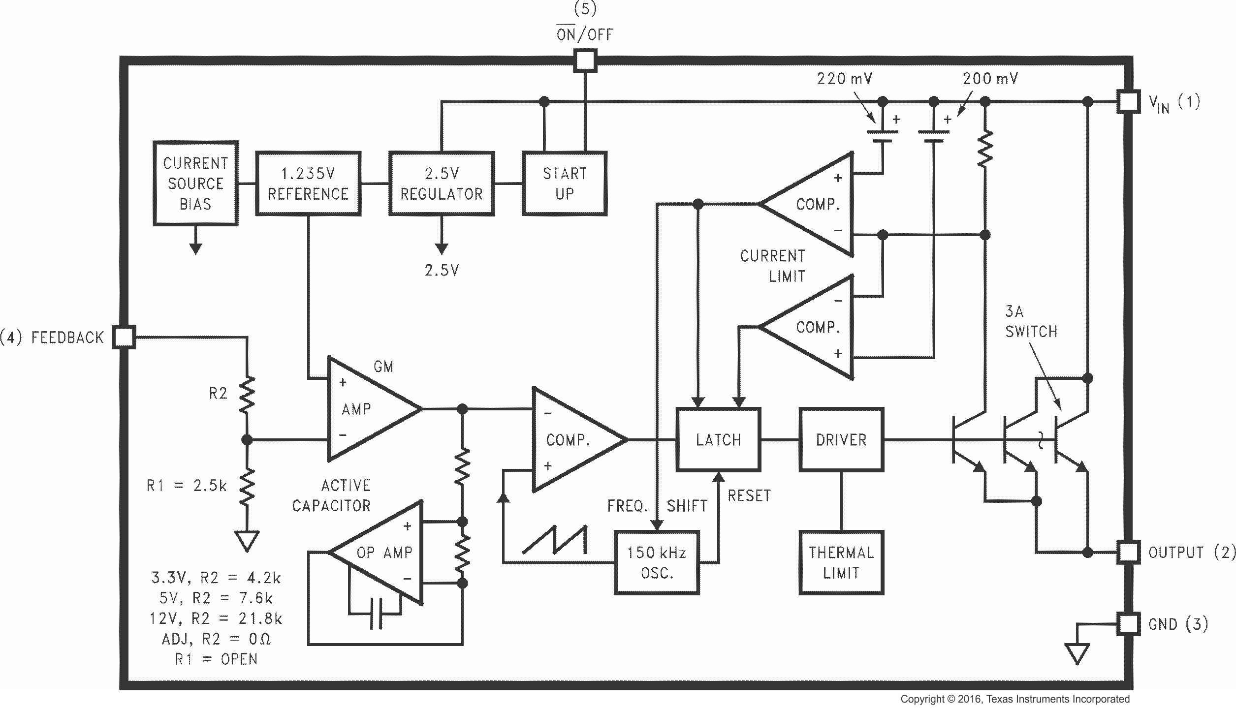
9.2 Functional Block Diagram

9.3 Feature Description
9.3.1 Delayed Start-Up
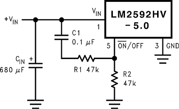
The circuit in Figure 21 uses the ON/OFF pin to provide a time delay between the time the input voltage is applied and the time the output voltage comes up (only the circuitry pertaining to the delayed start-up is shown). As the input voltage rises, the charging of capacitor C1 pulls the ON/OFF pin high, keeping the regulator off. When the input voltage reaches its final value and the capacitor stops charging, the resistor R2 pulls the ON/OFF pin low, thus allowing the circuit to start switching. Resistor R1 is included to limit the maximum voltage applied to the ON/OFF pin (maximum of 25 V), reduces power supply noise sensitivity, and also limits the capacitor, C1, discharge current. When high input ripple voltage exists, avoid long delay time, because this ripple can be coupled into the ON/OFF pin and cause problems.
This delayed start-up feature is useful in situations where the input power source is limited in the amount of current it can deliver. It allows the input voltage to rise to a higher voltage before the regulator starts operating. Buck regulators require less input current at higher input voltages.
 Figure 21. Delayed Start-Up
9.3.2 Undervoltage Lockout
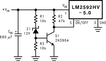
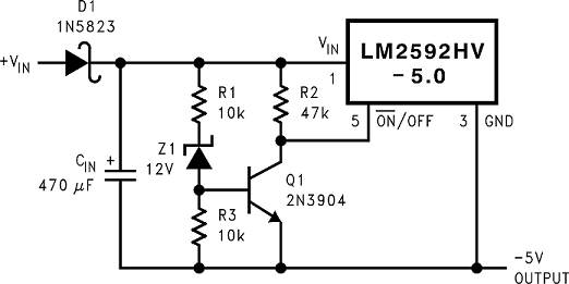
Some applications require the regulator to remain off until the input voltage reaches a predetermined voltage. An undervoltage lockout feature applied to a buck regulator is shown in Figure 22, while Figure 23 applies the same feature to an inverting circuit. The circuit in Figure 22 features a constant threshold voltage for turnon and turnoff (Zener voltage plus approximately one volt). The circuit in Figure 23 has a turnon threshold of about 13 V and a turnoff threshold of about 8 V. The amount of hysteresis is approximately equal to the output voltage. If Zener voltages greater than 25 V are used, an additional 47-kΩ resistor is needed from the ON/OFF pin to the ground pin to stay within the 25-V maximum limit of the ON/OFF pin.
 Figure 22. Undervoltage Lockout for Buck Regulator

Regulator starts switching at VIN = 13 V.
Regulator stops switching at VIN = 8 V
9.4 Device Functional Modes
9.4.1 Shutdown Mode
The ON/OFF pin provides electrical ON and OFF control for the LM2592HV. When the voltage of this pin is higher than 2 V, the device is shutdown mode. The typical standby current in this mode is 90 μA.
9.4.2 Active Mode
When the ON/OFF pin is left floating or pull below 0.6 V, the device will start switching and the output voltage will rise until it reaches a normal regulation voltage.