JAJS853C May 1999 – May 2016 LM2595
PRODUCTION DATA.
- 1 特長
- 2 アプリケーション
- 3 概要
- 4 改訂履歴
- 5 概要(続き)
- 6 Pin Configuration and Functions
-
7 Specifications
- 7.1 Absolute Maximum Ratings
- 7.2 ESD Ratings
- 7.3 Recommended Operating Conditions
- 7.4 Thermal Information
- 7.5 Electrical Characteristics - 3.3 V
- 7.6 Electrical Characteristics - 5 V
- 7.7 Electrical Characteristics - 12 V
- 7.8 Electrical Characteristics - Adjustable
- 7.9 Electrical Characteristics - All Output Voltage Versions
- 7.10 Typical Characteristics
- 8 Detailed Description
- 9 Application and Implementation
- 10Power Supply Recommendations
- 11Layout
- 12デバイスおよびドキュメントのサポート
- 13メカニカル、パッケージ、および注文情報
パッケージ・オプション
デバイスごとのパッケージ図は、PDF版データシートをご参照ください。
メカニカル・データ(パッケージ|ピン)
- NDH|5
- KTT|5
サーマルパッド・メカニカル・データ
発注情報
6 Pin Configuration and Functions
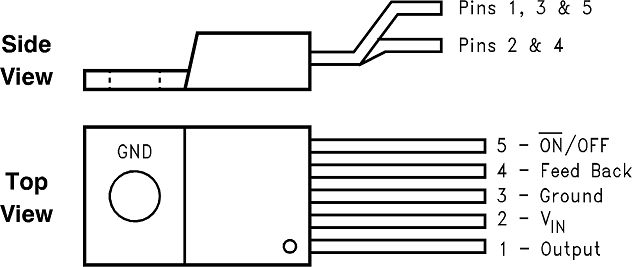
NDH Package
5–Pin TO-220
Top View

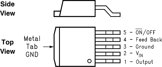
KTT Package
5-Pin TO-263
Top View

Pin Functions
| PIN | I/O | DESCRIPTION | |
|---|---|---|---|
| NO. | NAME | ||
| 1 | Output | O | Internal switch. The voltage at this pin switches between (+VIN − VSAT) and approximately –0.5 V, with a duty cycle of approximately VOUT/VIN. To minimize coupling to sensitive circuitry, the PCB copper area connected to this pin must be kept to a minimum. |
| 2 | +VIN | I | This is the positive input supply for the IC switching regulator. A suitable input bypass capacitor must be present at this pin to minimize voltage transients and to supply the switching currents needed by the regulator. |
| 3 | Ground | — | Circuit ground. |
| 4 | Feedback | I | Senses the regulated output voltage to complete the feedback loop. |
| 5 | ON/OFF | I | Allows the switching regulator circuit to be shut down using logic level signals, thus dropping the total input supply current to approximately 85 μA. Pulling this pin below a threshold voltage of approximately 1.3 V turns the regulator on, and pulling this pin above 1.3 V (up to a maximum of 25 V) shuts the regulator down. If this shutdown feature is not needed, the ON/OFF pin can be wired to the ground pin or it can be left open, in either case the regulator is in the ON condition. |