JAJS908F May 2004 – June 2016 LM2675
PRODUCTION DATA.
- 1 特長
- 2 アプリケーション
- 3 概要
- 4 改訂履歴
- 5 Description (continued)
- 6 Pin Configuration and Functions
-
7 Specifications
- 7.1 Absolute Maximum Ratings
- 7.2 ESD Ratings
- 7.3 Recommended Operating Conditions
- 7.4 Thermal Information
- 7.5 Electrical Characteristics - 3.3 V
- 7.6 Electrical Characteristics - 5 V
- 7.7 Electrical Characteristics - 12 V
- 7.8 Electrical Characteristics - Adjustable
- 7.9 Electrical Characteristics - All Output Voltage Versions
- 7.10 Typical Characteristics
- 7.11 Typical Characteristics - Fixed Output Voltage Versions
- 8 Detailed Description
- 9 Application and Implementation
- 10Power Supply Recommendations
- 11Layout
- 12デバイスおよびドキュメントのサポート
- 13メカニカル、パッケージ、および注文情報
8 Detailed Description
8.1 Overview
The LM2675 provides all of the active functions required for a step-down (buck) switching regulator. The internal power switch is a DMOS power MOSFET to provide power supply designs with high current capability, up to 1 A, and highly efficient operation. The LM2675 is part of the SIMPLE SWITCHER® family of power converters. A complete design uses a minimum number of external components, which have been predetermined from a variety of manufacturers. Using either this data sheet or TI's WEBENCH® design tool, a complete switching power supply can be designed quickly. See LM2670 SIMPLE SWITCHER® High Efficiency 3A Step-Down Voltage Regulator with Sync for additional application information.
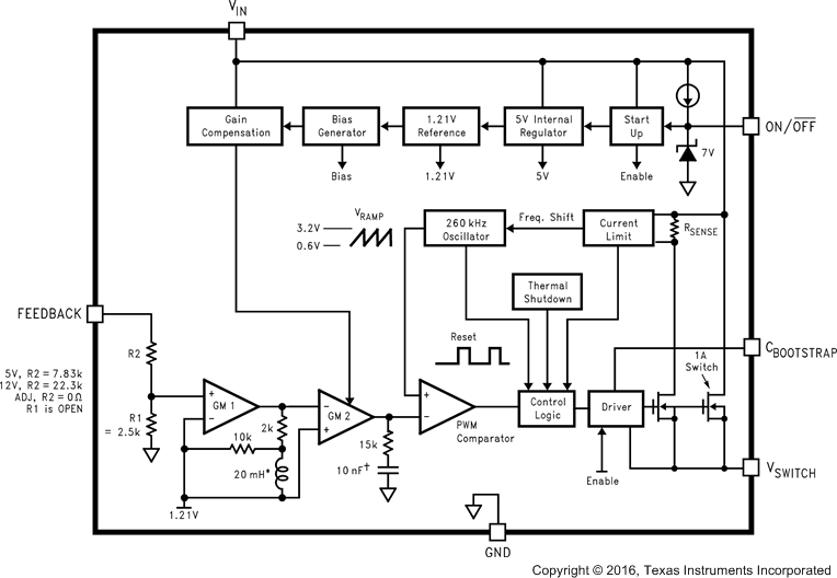
8.2 Functional Block Diagram

8.3 Feature Description
8.3.1 Adjustable Output Voltage
The voltage regulation loop in the LM2675 regulates output voltage by maintaining the voltage on FB pin (VFB) to be the same as the internal REF voltage (VREF). A resistor divider pair is needed to program the ratio from output voltage VOUT to VFB. The resistor is connected from the VOUT of the LM2674 to ground with the mid-point connecting to the FB pin. The voltage reference system produces a precise voltage reference over temperature. The internal REF voltage is typically 1.21 V. To program the output voltage of the LM2675 to be a certain value VOUT, R1 can be calculated with a selected R2. See Programming Output Voltage for adjustable output voltage typical application. The recommended range for R2 in most application is from 10 kΩ to 100 kΩ. If the resistor divider is not connected properly, output voltage cannot be regulated because the feedback loop is broken. If the FB pin is shorted to ground, the output voltage is driven close to VIN, because the regulator sees very low voltage on the FB pin and tries to regulate it. The load connected to the output could be damaged under such a condition. Do not short FB pin to ground when the LM2675 is enabled. It is important to route the feedback trace away from the noisy area of the PCB. For more layout recommendations, see Layout.
8.4 Device Functional Modes
8.4.1 Shutdown Mode
The ON/OFF pin provides electrical ON and OFF control for the LM2674. When the voltage of this pin is lower than 1.4 V, the device is in shutdown mode. The typical standby current in this mode is 20 μA.
8.4.2 Active Mode
When the voltage of the ON/OFF pin is higher than 1.4 V, the device starts switching and the output voltage rises until it reaches a normal regulation voltage.