JAJSG39 September   2018 LM2735-Q1

PRODUCTION DATA.  

  1. 特長
  2. アプリケーション
  3. 概要
    1.     Device Images
      1.      代表的な昇圧アプリケーションの回路
      2.      効率と負荷電流との関係VO=12V
  4. 改訂履歴
  5. Pin Configuration and Functions
    1.     Pin Functions
  6. Specifications
    1. 6.1 Absolute Maximum Ratings
    2. 6.2 ESD Ratings
    3. 6.3 Recommended Operating Conditions
    4. 6.4 Thermal Information
    5. 6.5 Electrical Characteristics
    6. 6.6 Typical Characteristics
  7. Detailed Description
    1. 7.1 Overview
      1. 7.1.1 Theory of Operation
    2. 7.2 Functional Block Diagram
    3. 7.3 Feature Description
      1. 7.3.1 Current Limit
      2. 7.3.2 Thermal Shutdown
      3. 7.3.3 Soft Start
      4. 7.3.4 Compensation
    4. 7.4 Device Functional Modes
      1. 7.4.1 Enable Pin and Shutdown Mode
  8. Application and Implementation
    1. 8.1 Application Information
    2. 8.2 Typical Applications
      1. 8.2.1  LM2735X-Q1 SOT-23 Design Example 1
        1. 8.2.1.1 Design Requirements
        2. 8.2.1.2 Detailed Design Procedure
          1. 8.2.1.2.1 Custom Design With WEBENCH® Tools
          2. 8.2.1.2.2 Inductor Selection
          3. 8.2.1.2.3 Input Capacitor
          4. 8.2.1.2.4 Output Capacitor
          5. 8.2.1.2.5 Setting the Output Voltage
        3. 8.2.1.3 Application Curves
      2. 8.2.2  LM2735Y-Q1 SOT-23 Design Example 2
      3. 8.2.3  LM2735X-Q1 WSON Design Example 3
      4. 8.2.4  LM2735Y-Q1 WSON Design Example 4
      5. 8.2.5  LM2735X-Q1 SOT-23 Design Example 6
      6. 8.2.6  LM2735Y-Q1 SOT-23 Design Example 7
      7. 8.2.7  LM2735X-Q1 SOT-23 Design Example 8
      8. 8.2.8  LM2735Y-Q1 SOT-23 Design Example 9
      9. 8.2.9  LM2735X-Q1 WSON Design Example 10
      10. 8.2.10 LM2735Y-Q1 WSON Design Example 11
      11. 8.2.11 LM2735X-Q1 WSON SEPIC Design Example 12
      12. 8.2.12 LM2735X-Q1 SOT-23 LED Design Example 14
      13. 8.2.13 LM2735Y-Q1 WSON FlyBack Design Example 15
      14. 8.2.14 LM2735X-Q1 SOT-23 LED Design Example 16 VRAIL > 5.5 V Application
      15. 8.2.15 LM2735X-Q1 SOT-23 LED Design Example 17 Two-Input Voltage Rail Application
      16. 8.2.16 SEPIC Converter
        1. 8.2.16.1 Detailed Design Procedure
          1. 8.2.16.1.1 SEPIC Design Guide
          2. 8.2.16.1.2 Small Ripple Approximation
          3. 8.2.16.1.3 Steady State Analysis With Loss Elements
  9. Power Supply Recommendations
  10. 10Layout
    1. 10.1 Layout Guidelines
      1. 10.1.1 WSON Package
    2. 10.2 Layout Examples
    3. 10.3 Thermal Considerations
      1. 10.3.1 Definitions
      2. 10.3.2 PCB Design With Thermal Performance in Mind
      3. 10.3.3 LM2735-Q1 Thermal Models
      4. 10.3.4 Calculating Efficiency, and Junction Temperature
        1. 10.3.4.1 Example Efficiency Calculation
      5. 10.3.5 Calculating RθJA and RΨJC
        1. 10.3.5.1 Procedure
        2. 10.3.5.2 Example From Previous Calculations
  11. 11デバイスおよびドキュメントのサポート
    1. 11.1 デバイス・サポート
      1. 11.1.1 デベロッパー・ネットワークの製品に関する免責事項
    2. 11.2 WEBENCH®ツールによるカスタム設計
    3. 11.3 ドキュメントのサポート
      1. 11.3.1 関連資料
    4. 11.4 ドキュメントの更新通知を受け取る方法
    5. 11.5 コミュニティ・リソース
    6. 11.6 商標
    7. 11.7 静電気放電に関する注意事項
    8. 11.8 Glossary
  12. 12メカニカル、パッケージ、および注文情報

パッケージ・オプション

メカニカル・データ(パッケージ|ピン)
サーマルパッド・メカニカル・データ
発注情報

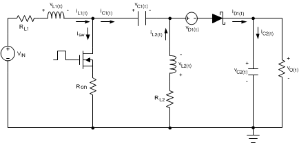
Steady State Analysis With Loss Elements

LM2735-Q1 20215866.gif

Using inductor volt-second balance and capacitor charge balance, the following equations are derived:

Equation 24. LM2735-Q1 20215867.gif
Equation 25. LM2735-Q1 20215868.gif

Therefore:

Equation 26. LM2735-Q1 20215869.gif

One can see that all variables are known except for the duty cycle (D). A quadratic equation is needed to solve for D. A less accurate method of determining the duty cycle is to assume efficiency, and calculate the duty cycle.

Equation 27. LM2735-Q1 20215870.gif
Equation 28. LM2735-Q1 20215871.gif
LM2735-Q1 20215890.gifFigure 39. Efficiencies for Typical SEPIC Application