SNOSC48O June 2000 – December 2014 LM2936
PRODUCTION DATA.
5 Pin Configuration and Functions
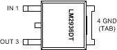
3-Pins
LM2936DT TO-252 (NDP) Package
Top View
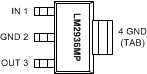
4-Pins
LM2936MP SOT-223 (DCY) Package
Top View
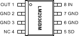
8-Pins
LM2936BM SOIC (D) Package
Top View
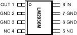
8-Pins
LM2936M SOIC (D) Package
Top View
3-Pins
LM2936Z TO-92 (LP) Package
Bottom View

8-Pins
LM2936MM VSSOP (DGK) Package
Top View
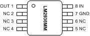
Pin Functions
| PIN | I/O | DESCRIPTION | ||||||
|---|---|---|---|---|---|---|---|---|
| NAME | D (LM2936BM) |
D (LM2936M) |
NDP | DGK | DCY | LP | ||
| IN | 8 | 8 | 1 | 8 | 1 | 3 | I | Unregulated input voltage. |
| GND | 2, 3, 6, 7 | 2, 3, 6, 7 | 4 | 7 | 2, 4 | 2 | — | Ground. |
| OUT | 1 | 1 | 3 | 1 | 3 | 1 | O | Regulated output voltage. Requires a minimum output capacitance, with specific ESR, on this pin to maintain stability. |
| SD | 5 | — | — | — | — | — | I | Shutdown. LM2936BM only. Pull this pin HIGH (> 2 V) to turn the output OFF. If this pin is left open, pull ed low (< 0.6 V), or connected to GND, the output will be ON by default. Avoid having any voltage between 0.6 V and 2 V on this pin as the output status may not be predicable across the operating range. |
| NC | 4 | 4, 5 | — | 2, 3, 4, 5, 6 | — | — | — | No internal connection, Connect to GND, or leave open. |