SNOS935C February 2001 – December 2014 LM321
PRODUCTION DATA.
- 1 Features
- 2 Applications
- 3 Description
- 4 Revision History
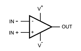
- 5 Pin Configuration and Functions
- 6 Specifications
- 7 Detailed Description
- 8 Application and Implementation
- 9 Power Supply Recommendations
- 10Layout
- 11Device and Documentation Support
- 12Mechanical, Packaging, and Orderable Information
7 Detailed Description
7.1 Overview
The LM321 operational amplifer can operate with a single or dual power supply voltage, has true-differential inputs, and remains in the linear mode with an input common-mode voltage of 0 VDC. This amplifier operates over a wide range of power supply voltages, with little change in performance characteristics. At 25°C amplifier operation is possible down to a minimum supply voltage of 3 V. Large differential input voltages can be easily accommodated and, as input differential voltage protection diodes are not needed, no large input currents result from large differential input voltages. The differential input voltage may be larger than V+ without damaging the device. Protection should be provided to prevent the input voltages from going negative more than −0.3 VDC (at 25°C). An input clamp diode with a resistor to the IC input terminal can be used.
7.2 Functional Block Diagram
7.3 Feature Description
To reduce the power supply drain, the amplifier has a class A output stage for small signal levels which converts to class B in a large signal mode. This allows the amplifiers to both source and sinks large output currents. Therefore both NPN and PNP external current boost transistors can be used to extend the power capability of the basic amplifiers. The output voltage needs to raise approximately 1 diode drop above ground to bias the on chip vertical PNP transistor for output current sinking applications.
For AC applications, where the load is capacitively coupled to the output of the amplifier, a resistor should be used, from the output of the amplifier to ground to increase the class A bias current and to reduce distortion.
Capacitive loads which are applied directly to the output of the amplifier reduce the loop stability margin. Values of 50 pF can be accommodated using the worst-case non-inverting unity gain connection. Large closed loop gains or resistive isolation should be used if large load capacitance must be driven by the amplifier.
The bias network of the LM321 establishes a supply current which is independent of the magnitude of the power supply voltage over the range of from 3 VDC to 30 VDC.
Output short circuits either to ground or to the positive power supply should be of short time duration. Units can be destroyed, not as a result of the short circuit current causing metal fusing, but rather due to the large increase in IC chip dissipation which will cause eventual failure due to excessive junction temperatures. The larger value of output source current which is available at 25°C provides a larger output current capability at elevated temperatures than a standard IC operational amplifer.
7.4 Device Functional Modes
7.4.1 Common-Mode Voltage Range
The input common-mode voltage range of the LM321 series extends from 300 mV below ground to 32 V for normal operation. The typical performance in this range is summarized in Table 1:
Table 1. Typical Performance Range (Vs = 5 V)
| PARAMETER | MIN | TYP | MAX | UNIT |
|---|---|---|---|---|
| Input voltage range | –0.3 | 32 | V | |
| Offset voltage | 2 | 7 | mV | |
| Offset voltage drift (TA = –40°C to 85°C) | 9 | µV/°C | ||
| CMRR | 65 | 85 | dB | |
| PSRR | 65 | 100 | dB | |
| Gain bandwidth product (GBP) | 1 | MHz | ||
| Slew rate | 0.4 | V/µs | ||
| Phase margin | 60 | ° | ||
| Equivalent input noise voltage | 40 | nV/√Hz |