JAJS711X July 2000 – June 2017 LM3478
PRODUCTION DATA.
- 1 特長
- 2 アプリケーション
- 3 説明
- 4 改訂履歴
- 5 Pin Configuration and Functions
- 6 Specifications
- 7 Detailed Description
-
8 Application and Implementation
- 8.1 Application Information
- 8.2
Typical Applications
- 8.2.1
Typical High Efficiency Step-Up (Boost) Converter
- 8.2.1.1 Design Requirements
- 8.2.1.2
Detailed Design Procedure
- 8.2.1.2.1 Custom Design with WEBENCH Tools
- 8.2.1.2.2 Power Inductor Selection
- 8.2.1.2.3 Programming the Output Voltage
- 8.2.1.2.4 Setting the Current Limit
- 8.2.1.2.5 Current Limit with External Slope Compensation
- 8.2.1.2.6 Power Diode Selection
- 8.2.1.2.7 Power MOSFET Selection
- 8.2.1.2.8 Input Capacitor Selection
- 8.2.1.2.9 Output Capacitor Selection
- 8.2.1.2.10 Compensation
- 8.2.1.3 Application Curves
- 8.2.2 Typical SEPIC Converter
- 8.2.1
Typical High Efficiency Step-Up (Boost) Converter
- 9 Power Supply Recommendations
- 10Layout
- 11デバイスおよびドキュメントのサポート
- 12メカニカル、パッケージ、および注文情報
パッケージ・オプション
メカニカル・データ(パッケージ|ピン)
サーマルパッド・メカニカル・データ
発注情報
7 Detailed Description
7.1 Overview
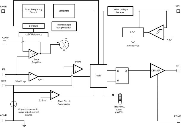
The LM3478 device uses a fixed frequency, Pulse Width Modulated (PWM) current mode control architecture. The Functional Block Diagram shows the basic functionality. In a typical application circuit, the peak current through the external MOSFET is sensed through an external sense resistor. The voltage across this resistor is fed into the ISEN pin. This voltage is fed into the positive input of the PWM comparator. The output voltage is also sensed through an external feedback resistor divider network and fed into the error amplifier negative input (feedback pin, FB). The output of the error amplifier (COMP pin) is added to the slope compensation ramp and fed into the negative input of the PWM comparator. At the start of any switching cycle, the oscillator sets the RS latch using the switch logic block. This forces a high signal on the DR pin (gate of the external MOSFET) and the external MOSFET turns on. When the voltage on the positive input of the PWM comparator exceeds the negative input, the RS latch is reset and the external MOSFET turns off.
The voltage sensed across the sense resistor generally contains spurious noise spikes, as shown in Figure 20. These spikes can force the PWM comparator to reset the RS latch prematurely. To prevent these spikes from resetting the latch, a blank-out circuit inside the IC prevents the PWM comparator from resetting the latch for a short duration after the latch is set. This duration is about 325 ns and is called the blanking interval and is specified as minimum on-time in the Electrical Characteristics section. Under extremely light-load or no-load conditions, the energy delivered to the output capacitor when the external MOSFET in on during the blanking interval is more than what is delivered to the load. An over-voltage comparator inside the LM3478 prevents the output voltage from rising under these conditions. The over-voltage comparator senses the feedback (FB pin) voltage and resets the RS latch. The latch remains in reset state until the output decays to the nominal value.
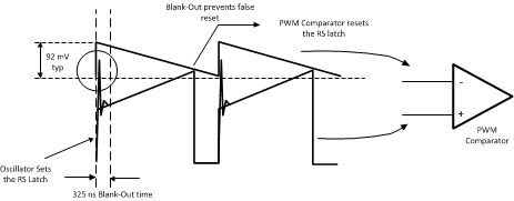 Figure 20. Basic Operation of the PWM Comparator
7.2 Functional Block Diagram
7.3 Feature Description
7.3.1 Overvoltage Protection
The LM3478 has over voltage protection (OVP) for the output voltage. OVP is sensed at the feedback pin (pin 3). If at anytime the voltage at the feedback pin rises to VFB+ VOVP, OVP is triggered. See Electrical Characteristics section for limits on VFB and VOVP.
OVP will cause the drive pin to go low, forcing the power MOSFET off. With the MOSFET off, the output voltage will drop. The LM3478 will begin switching again when the feedback voltage reaches VFB + (VOVP - VOVP(HYS)). See Electrical Characteristics for limits on VOVP(HYS).
OVP can be triggered if the unregulated input voltage crosses 7.2 V, the output voltage will react as shown in Figure 21. The internal bias of the LM3478 comes from either the internal LDO as shown in the block diagram or the voltage at the Vin pin is used directly. At Vin voltages lower than 7.2 V the internal IC bias is the Vin voltage and at voltages above 7.2V the internal LDO of the LM3478 provides the bias. At the switch over threshold at 7.2 V a sudden small change in bias voltage is seen by all the internal blocks of the LM3478. The control voltage shifts because of the bias change, the PWM comparator tries to keep regulation. To the PWM comparator, the scenario is identical to a step change in the load current, so the response at the output voltage is the same as would be observed in a step load change. Hence, the output voltage overshoot here can also trigger OVP. The LM3478 will regulate in hysteretic mode for several cycles, or may not recover and simply stay in hysteretic mode until the load current drops or Vin is not crossing the 7.2 V threshold anymore. Note that the output is still regulated in hysteretic mode.
Depending on the requirements of the application, there is some influence one has over this effect. The threshold of 7.2 V can be shifted to higher voltages by adding a resistor in series with VIN. In case VIN is right at the threshold of 7.2 V, the threshold could cross over and over due to some slight ripple on VIN. To minimize the effect on the output voltage one can filter the VIN pin with an RC filter.
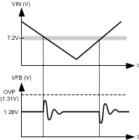 Figure 21. The Feedback Voltage Experiences an Oscillation if the Input Voltage crosses the 7.2-V Internal Bias Threshold
7.3.2 Slope Compensation Ramp
The LM3478 uses a current mode control scheme. The main advantages of current mode control are inherent cycle-by-cycle current limit for the switch and simpler control loop characteristics. It is also easy to parallel power stages using current mode control since current sharing is automatic. However, current mode control has an inherent instability for duty cycles greater than 50%, as shown in Figure 22.
A small increase in the load current causes the switch current to increase by ΔI0. The effect of this load change is ΔI1.
The two solid waveforms shown are the waveforms compared at the internal pulse width modulator, used to generate the MOSFET drive signal. The top waveform with the slope Se is the internally generated control waveform VC. The bottom waveform with slopes Sn and Sf is the sensed inductor current waveform VSEN.
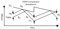 Figure 22. Sub-Harmonic Oscillation for D>0.5 and Compensation Ramp to Avoid Sub-Harmonic Oscillation
Sub-harmonic Oscillation can be easily understood as a geometric problem. If the control signal does not have slope, the slope representing the inductor current ramps up until the control signal is reached and then slopes down again. If the duty cycle is above 50%, any perturbation will not converge but diverge from cycle to cycle and causes sub-harmonic oscillation.
It is apparent that the difference in the inductor current from one cycle to the next is a function of Sn, Sf and Se as shown in Equation 1.

Hence, if the quantity (Sf - Se)/(Sn + Se) is greater than 1, the inductor current diverges and sub-harmonic oscillation results. This counts for all current mode topologies. The LM3478 has some internal slope compensation VSL which is enough for many applications above 50% duty cycle to avoid sub-harmonic oscillation .
For boost applications, the slopes Se, Sf and Sn can be calculated with Equation 2, Equation 3, and Equation 4.
When Se increases, then the factor that determines if sub-harmonic oscillation will occur decreases. When the duty cycle is greater than 50%, and the inductance becomes less, the factor increases.
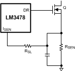
For more flexibility, slope compensation can be increased by adding one external resistor, RSL, in the ISEN's path. Figure 23 shows the setup. The externally generated slope compensation is then added to the internal slope compensation of the LM3478. When using external slope compensation, the formula for Se becomes:
A typical value for factor K is 40 µA.
The factor changes with switching frequency. Figure 24 is used to determine the factor K for individual applications and Equation 6 gives the factor K.
It is a good design practice to only add as much slope compensation as needed to avoid sub-harmonic oscillation. Additional slope compensation minimizes the influence of the sensed current in the control loop. With very large slope compensation the control loop characteristics are similar to a voltage mode regulator which compares the error voltage to a saw tooth waveform rather than the inductor current.
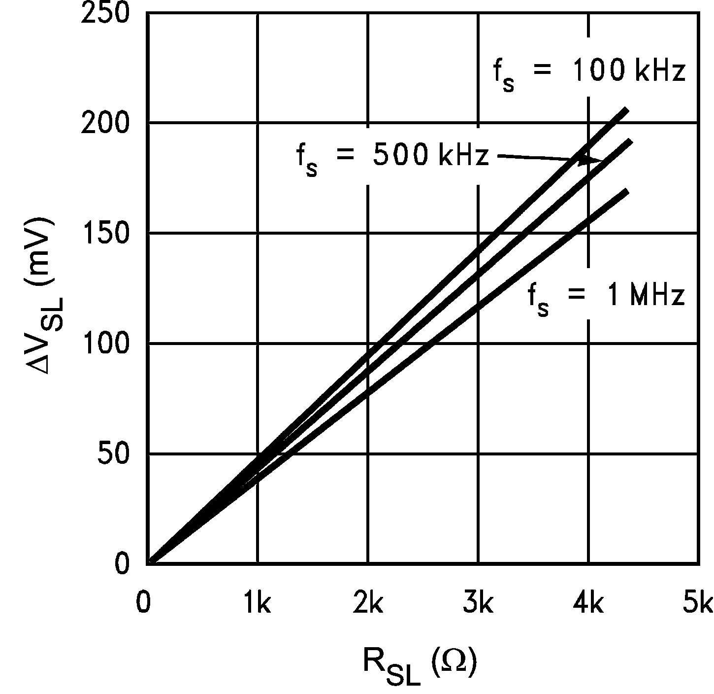
ΔVSL vs RSL
7.3.3 Frequency Adjust/Shutdown
The switching frequency of the LM3478 can be adjusted between 100 kHz and 1 MHz using a single external resistor. This resistor must be connected between FA/SD pin and ground, as shown in Figure 25. To determine the value of the resistor required for a desired switching frequency, refer to Typical Characteristics or use Equation 7:
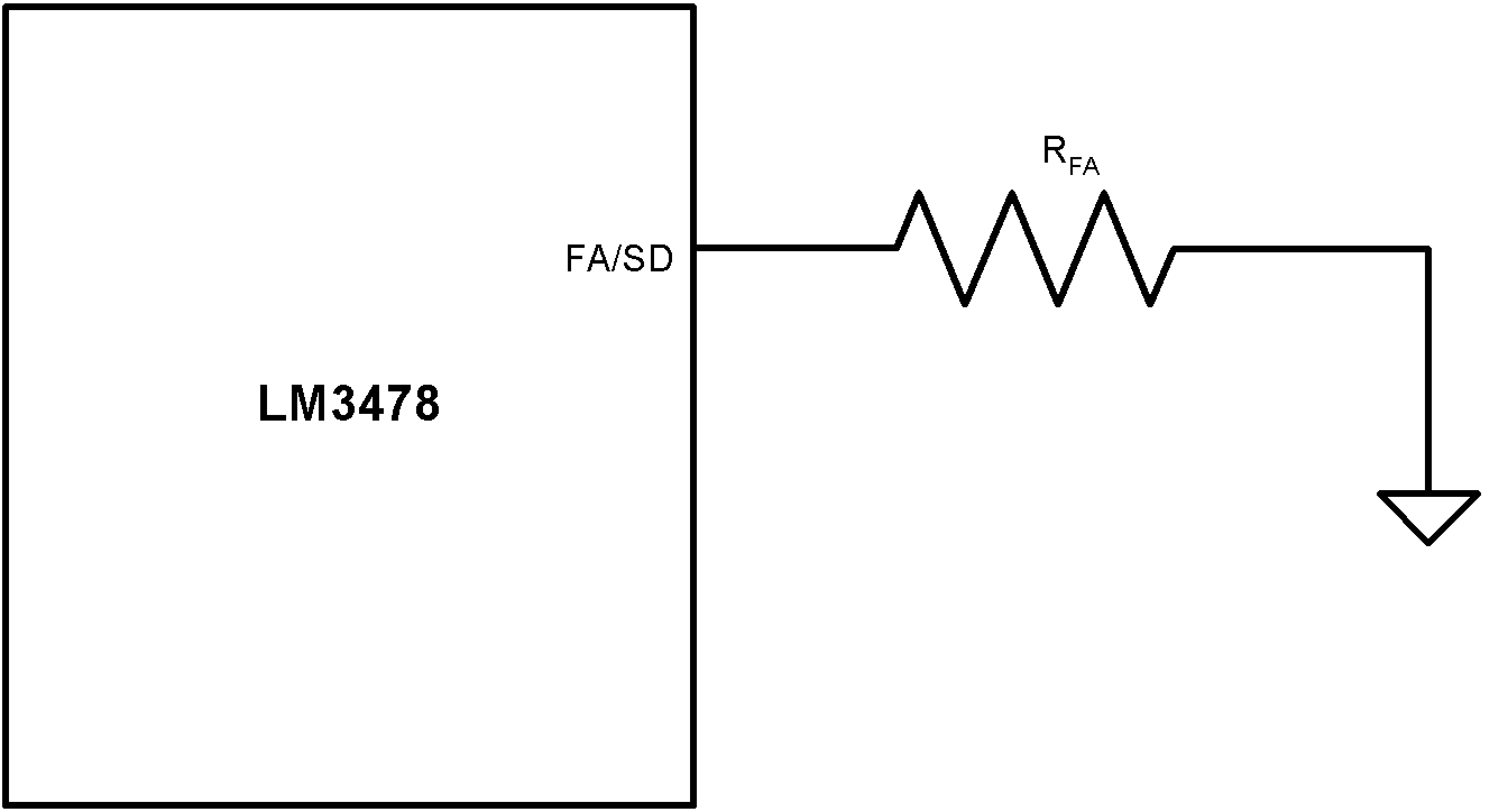 Figure 25. Frequency Adjust
The FA/SD pin also functions as a shutdown pin. If a high signal (>1.35 V) appears on the FA/SD pin, the LM3478 stops switching and goes into a low current mode. The total supply current of the IC reduces to less than 10 µA under these conditions. Figure 26 shows implementation of the shutdown function when operating in frequency adjust mode. In this mode a high signal for more than 30 us shuts down the IC. However, the voltage on the FA/SD pin should be always less than the absolute maximum of 7 V to avoid any damage to the device.
 Figure 26. Shutdown Operation in Frequency Adjust Mode
7.3.4 Short-Circuit Protection
When the voltage across the sense resistor measured on the ISEN pin exceeds 343 mV, short circuit current limit protection gets activated. A comparator inside the LM3478 reduces the switching frequency by a factor of 5 and maintains this condition until the short is removed. In normal operation the sensed current will trigger the power MOSFET to turn off. During the blanking interval the PWM comparator will not react to an over current so that this additional 343 mV current limit threshold is implemented to protect the device in a short circuit or severe overload condition.
7.4 Device Functional Modes
The device is set to run as soon as the input voltage crosses above the UVLO set point and at a frequency set according to the FA/SD pin pulldown resistor. If the FA/SD pin is pulled high, the LM3481 enters shut-down mode.