SNVS533D September 2007 – November 2014 LM4510
PRODUCTION DATA.
- 1 Features
- 2 Applications
- 3 Description
- 4 Revision History
- 5 Pin Configuration and Functions
- 6 Specifications
- 7 Detailed Description
-
8 Application and Implementation
- 8.1 Application Information
- 8.2
Typical Applications
- 8.2.1
2.7 V to 5.5 V Input with a 16 V Output
- 8.2.1.1 Design Requirements
- 8.2.1.2
Detailed Design Procedure
- 8.2.1.2.1 Adjusting Output Voltage
- 8.2.1.2.2 Maximum Output Current
- 8.2.1.2.3 Inductor Selection
- 8.2.1.2.4 IL_AVE Check
- 8.2.1.2.5 Input Capacitor Selection
- 8.2.1.2.6 Output Capacitor Selection
- 8.2.1.2.7 Soft-Start Function and Soft-Start Capacitor Selection
- 8.2.1.2.8 Compensation Component Selection
- 8.2.1.3 Application Curves
- 8.2.2 Flash and Torch Application
- 8.2.1
2.7 V to 5.5 V Input with a 16 V Output
- 9 Power Supply Recommendations
- 10Layout
- 11Device and Documentation Support
- 12Mechanical, Packaging, and Orderable Information
パッケージ・オプション
メカニカル・データ(パッケージ|ピン)
- DSC|10
サーマルパッド・メカニカル・データ
- DSC|10
発注情報
6 Specifications
6.1 Absolute Maximum Ratings(1)(2)(11)
| MIN | MAX | UNIT | |||
|---|---|---|---|---|---|
| VIN | −0.3 | 6.5 | V | ||
| VOUT | −0.3 | 21 | V | ||
| SW(3) | –0.3 | VOUT+0.3 | V | ||
| EN, SS, COMP FB | −0.3 | 6.5 | V | ||
| PGND to AGND | −0.2 | 0.2 | V | ||
| Continuous power dissipation(4) | Internally Limited | ||||
| Junction temperature (TJ-MAX) | 150 | 150 | °C | ||
| Lead temperature (soldering, 10 sec)(5) | 260 | °C | |||
6.2 Handling Ratings
| MIN | MAX | UNIT | |||
|---|---|---|---|---|---|
| Tstg | Storage temperature range | –65 | 150 | °C | |
| V(ESD) | Electrostatic discharge | Human body model (HBM), per ANSI/ESDA/JEDEC JS-001, all pins(1) | 2 | kV | |
| Charged device model (CDM), per JEDEC specification JESD22-C101, all pins(2) | 1000 | V | |||
| Machine model | 200 | V | |||
(1) JEDEC document JEP155 states that 500-V HBM allows safe manufacturing with a standard ESD control process.
(2) JEDEC document JEP157 states that 250-V CDM allows safe manufacturing with a standard ESD control process.
6.3 Recommended Operating Conditions
| MIN | MAX | UNIT | |||
|---|---|---|---|---|---|
| Supply voltage (VIN) | 2.7 | 5.5 | V | ||
| Junction temperature (TJ)(6) | −40 | 125 | °C | ||
| Output voltage (VOUT) | 18 | V | |||
6.4 Thermal Information
| THERMAL METRIC(1) | LM4510 | UNIT | |
|---|---|---|---|
| DSC | |||
| 10 PINS | |||
| RθJA | Junction-to-ambient thermal resistance | 36 | °C/W |
| RθJC(top) | Junction-to-case (top) thermal resistance | 48.3 | |
| RθJB | Junction-to-board thermal resistance | 22 | |
| ψJT | Junction-to-top characterization parameter | 0.6 | |
| ψJB | Junction-to-board characterization parameter | 22.1 | |
| RθJC(bot) | Junction-to-case (bottom) thermal resistance | 3.8 | |
(1) For more information about traditional and new thermal metrics, see the IC Package Thermal Metrics application report, SPRA953.
6.5 Electrical Characteristics
Unless otherwise stated the following conditions apply: VIN = 3.6 V, EN = 3.6 V, TJ = 25°C.| PARAMETER | TEST CONDITIONS | MIN(7) | TYP(8) | MAX(7) | UNIT | |
|---|---|---|---|---|---|---|
| VFB | FB Pin Voltage | 2.7 V ≤ VIN ≤ 5.5 V | 1.265 | V | ||
| 2.7 V ≤ VIN ≤ 5.5 V, −40°C ≤ TJ ≤ 125°C | 1.24 | 1.29 | ||||
| IFB | FB Pin Bias Current(10) | −40°C ≤ TJ ≤ 125°C | 0.050 | 1.5 | µA | |
| RDS(on) | NMOS Switch RDS(on) | ISW = 0.3 A | 0.45 | 1.1 | Ω | |
| PMOS Switch RDS(on) | ISW = 0.3 A, VOUT = 10 V | 0.9 | 1.1 | |||
| ICL | NMOS Switch Current Limit | 1 | 1.2 | 1.8 | A | |
| IQ | Device Switching | EN = 3.6 V, FB = COMP | 1.7 | mA | ||
| EN = 3.6 V, FB = COMP, −40°C ≤ TJ ≤ 125°C | 2.5 | |||||
| Non-switching Current | EN = 3.6 V, FB > 1.29 V | 0.8 | ||||
| EN = 3.6 V, FB > 1.29 V, −40°C ≤ TJ ≤ 125°C | 2 | |||||
| Shutdown Current | EN = 0 V | 0.002 | 0.050 | µA | ||
| IL | SW Leakage Current(10) | SW = 20 V | 0.01 | 0.150 | µA | |
| IVOUT | VOUT Bias Current(10) | VOUT = 20 V | 90 | µA | ||
| VOUT = 20 V, −40°C ≤ TJ ≤ 125°C | 50 | 150 | ||||
| IVL | PMOS Switch Leakage Current | SW = 0 V, VOUT = 20 V | 0.001 | 0.100 | µA | |
| fSW | Switching Frequency | 1 | MHz | |||
| −40°C ≤ TJ ≤ 125°C | 0.85 | 1.2 | ||||
| DMAX | Maximum Duty Cycle | FB = 0 V | 94% | |||
| FB = 0 V, −40°C ≤ TJ ≤ 125°C | 88% | |||||
| DMIN | Minimum Duty Cycle | 15% | 20% | |||
| Gm | Error Amplifier Transconductance | 130 | µmho | |||
| −40°C ≤ TJ ≤ 125°C | 70 | 200 | ||||
| EN Threshold |
Device Enable | HIGH | 0.81 | V | ||
| HIGH, −40°C ≤ TJ ≤ 125°C | 1.2 | |||||
| Device Shutdown | LOW | 0.78 | ||||
| LOW, −40°C ≤ TJ ≤ 125°C | 0.4 | |||||
| IEN | EN Pin Bias Current | 0 < EN < 3.6 V | 3.2 | µA | ||
| 0 < EN < 3.6 V, −40°C ≤ TJ ≤ 125°C | 8 | |||||
| FB Fault Protection | Feedback Fault Protection | ON Threshold | 19.7 | V | ||
| ON Threshold, −40°C ≤ TJ ≤ 125°C | 18 | 20.7 | ||||
| OFF Threshold | 18.7 | |||||
| OFF Threshold, −40°C ≤ TJ ≤ 125°C | 17 | 20 | ||||
| UVLO | Input Undervoltage Lockout | ON Threshold | 2.5 | V | ||
| ON Threshold, −40°C ≤ TJ ≤ 125°C | 2.65 | |||||
| OFF Threshold | 2.35 | |||||
| OFF Threshold, −40°C ≤ TJ ≤ 125°C | 2.1 | |||||
| ISS | Soft-Start Pin Current(9) | 11.3 | µA | |||
| −40°C ≤ TJ ≤ 125°C | 9 | 15 | ||||
(1) Absolute maximum ratings are limits beyond which damage to the device may occur. Recommended Operating Conditions are conditions for which the device is intended to be functional. For specifications and test conditions, see the Electrical Characteristics.
(2) All voltages are with respect to the potential at the GND pin.
(3) This condition applies if VIN < VOUT. If VIN > VOUT, a voltage greater than VIN + 0.3 V should not be applied to the VOUT or SW pins. The absolute maximum specification applies to DC voltage. An extended negative voltage limit of –1 V applies for a pulse of up to 1 µs, and –2 V for a pulse of up to 40 ns. An extended positive voltage limit of 22 V applies for a pulse of up to 20 ns.
(4) Internal thermal shutdown circuitry protects the device from permanent damage. Thermal shutdown engages at TJ= 150°C (Typ.) and disengages at TJ= 140°C (Typ.).
(5) For detailed soldering information and specifications, please refer to Application Note 1187: Leadless Leadframe Package (LLP) (SNOI401).
(6) In applications where high power dissipation and/or poor package thermal resistance is present, the maximum ambient temperature may have to be derated. Maximum ambient temperature (TA-MAX) is dependent on the maximum operating junction temperature (TJ-MAX-OP = 125°C), the maximum power dissipation of the device in the application (PD-MAX), and the junction-to ambient thermal resistance of the part/package in the application (RθJA), as given by the following equation: TA-MAX = TJ-MAX-OP – (RθJA × PD-MAX)
(7) All room temperature limits are production tested, specified through statistical analysis or by design. All limits at −40°C ≤ TJ ≤ 125°C are specified via correlation using standard Statistical Quality Control (SQC) methods. All limits are used to calculate Average Outgoing Quality Level (AOQL).
(8) Typical numbers are at 25°C and represent the most likely norm.
(9) Current flows out of the pin.
(10) Current flows into the pin.
(11) If Military/Aerospace specified devices are required, please contact the Texas Instruments Sales Office/ Distributors for availability and specifications.
6.6 Typical Characteristics
LM4510SD, Circuit of Figure 18, (L = 4.7 µH, COILCRAFT, DO3316-472ML; CIN = 4 .7 µF, TDK, C2012X5R0J475K; COUT = 10 µF, AVX, 12103D106KAT2A; CS = 10 nF, TDK, C1608C0G1E103J; CC1 = 2.2 nF, Taiyo Yuden, TMK107SD222JA-T; RC = 46.4 kΩ, Yageo, 9t06031A4642FBHFT), VIN = 3.6 V, VOUT = 16 V, TA = 25°C, unless otherwise noted.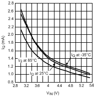 Figure 1. Switching Quiescent Current vs VIN
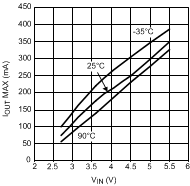 Figure 3. Load Capability vs VIN (VOUT = 16 V )
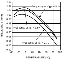 Figure 5. Switching Frequency vs Temperature
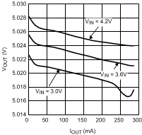 Figure 7. Load Regulation (VOUT = 5 V)
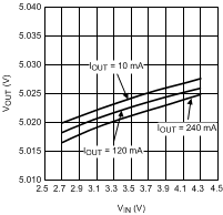
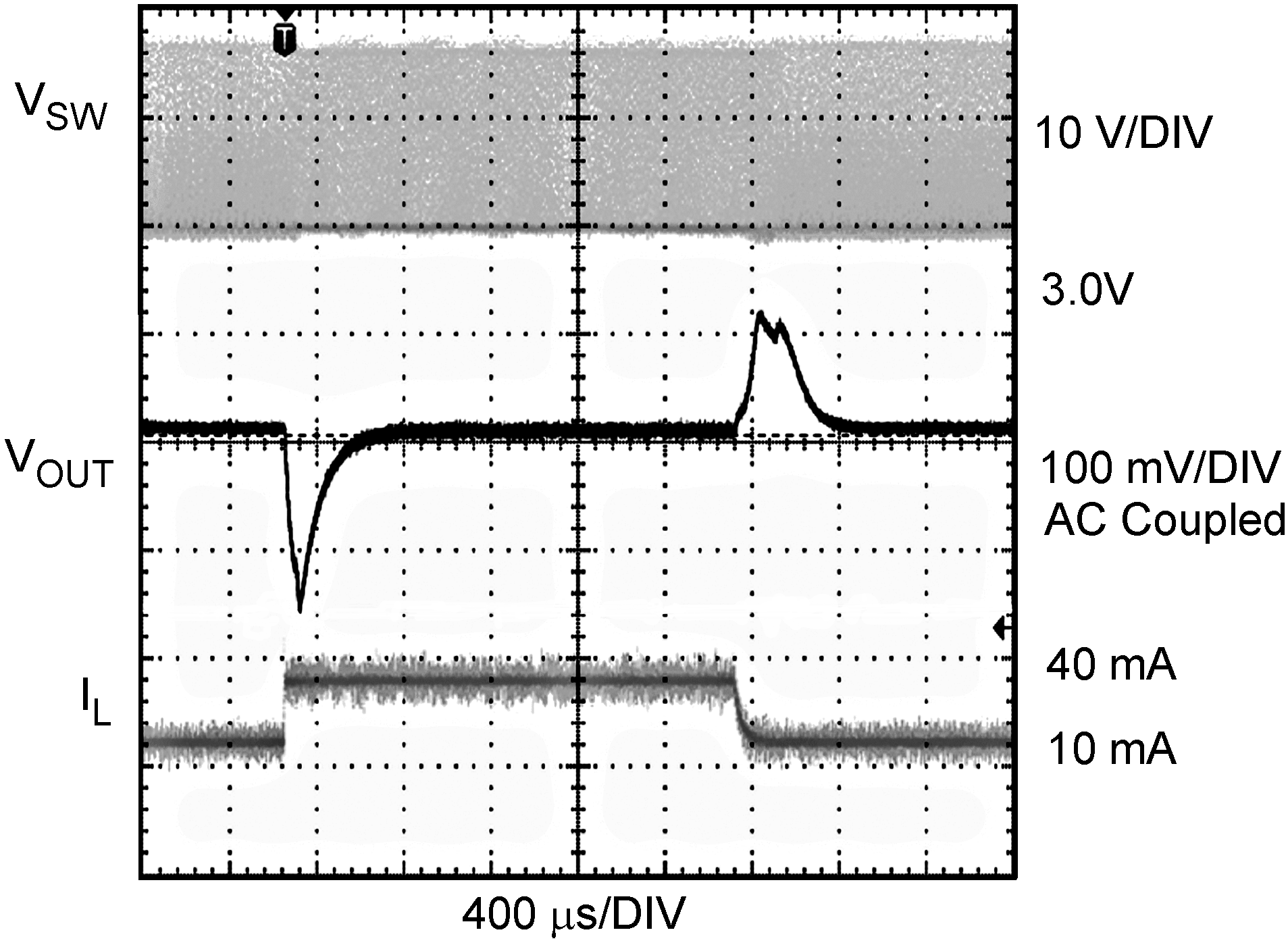 Figure 11. Load Transient Response (VOUT = 16 V)
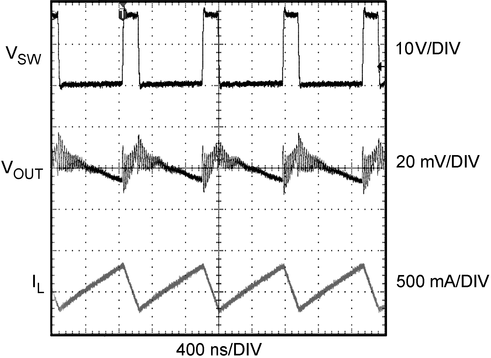 Figure 13. Output Voltage Ripple (VOUT = 16 V, IOUT = 90 mA)
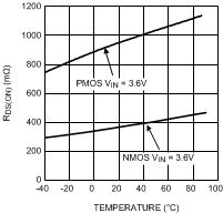 Figure 2. RDS(on) vs Temperature at VIN= 3.6 V
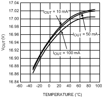 Figure 4. Output Voltage vs Temperature (VOUT = 17 V)
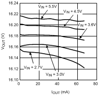 Figure 6. Load Regulation (VOUT = 16 V)
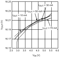 Figure 8. Line Regulation (VOUT = 16 V)
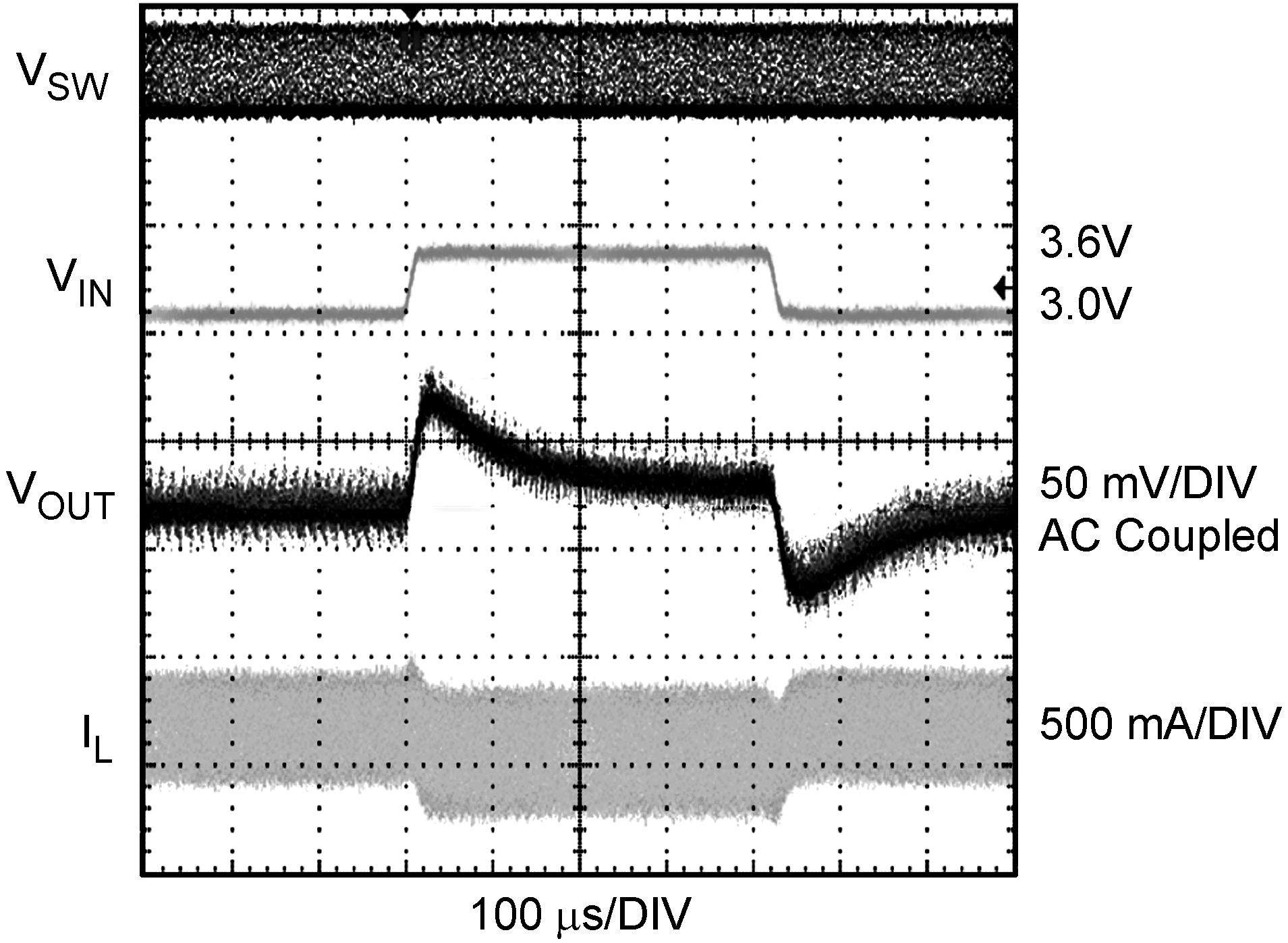 Figure 10. Line Transient Response (VOUT = 16 V)
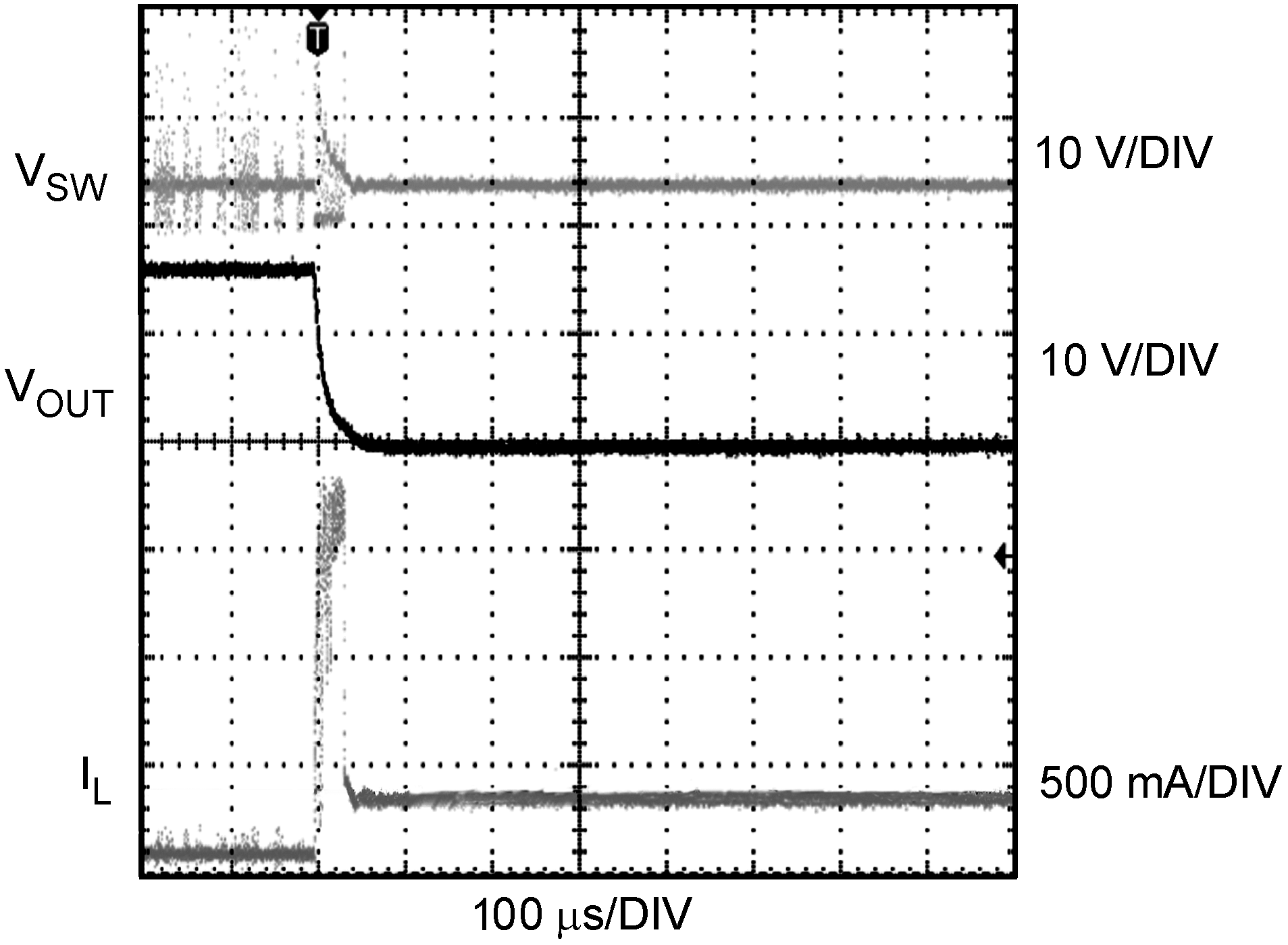 Figure 12. Short Circuit Response (VOUT = 16 V)
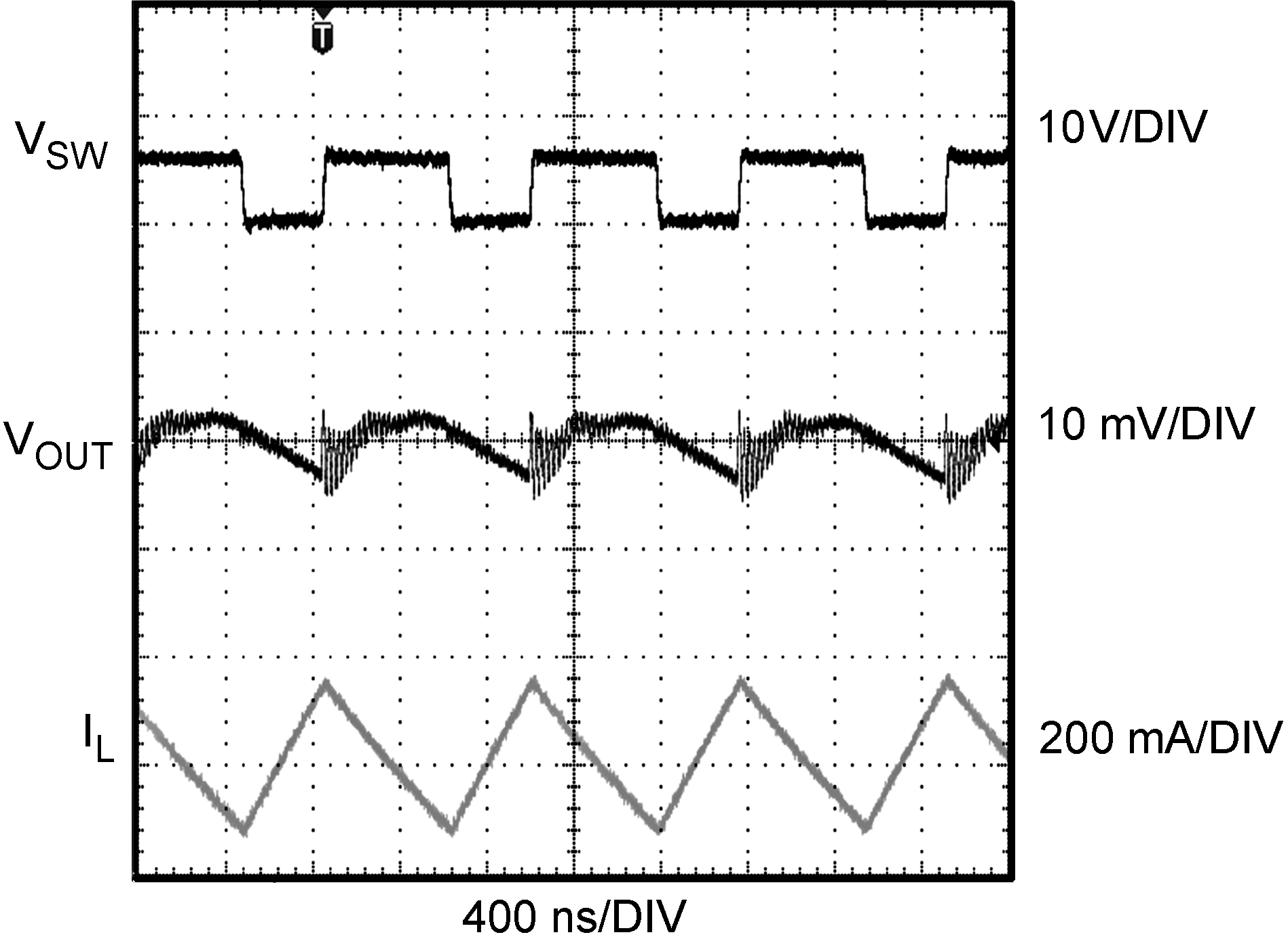 Figure 14. Output Voltage Ripple (VOUT = 5 V, IOUT = 100 mA)