SNVS344B March 2005 – December 2014 LM5032
PRODUCTION DATA.
- 1 Features
- 2 Applications
- 3 Description
- 4 Revision History
- 5 Pin Configuration and Functions
- 6 Specifications
-
7 Detailed Description
- 7.1 Overview
- 7.2 Functional Block Diagram
- 7.3
Feature Description
- 7.3.1 Line Undervoltage Lock Out, UVLO, Shutdown
- 7.3.2 Startup Regulator, VIN, VCC
- 7.3.3 Drivers Off, VCC Disable
- 7.3.4 Oscillator
- 7.3.5 PWM Comparator/Slope Compensation
- 7.3.6 Cycle-by-Cycle Current Limit
- 7.3.7 Hiccup Mode Current Limit Restart
- 7.3.8 Soft-Start
- 7.3.9 Output Duty Cycle
- 7.3.10 Driver Outputs
- 7.3.11 Thermal Shutdown
- 7.4 Device Functional Modes
-
8 Application and Implementation
- 8.1 Application Information
- 8.2 Typical Application
- 9 Power Supply Recommendations
- 10Layout
- 11Device and Documentation Support
- 12Mechanical, Packaging, and Orderable Information
6 Specifications
6.1 Absolute Maximum Ratings(5)(4)
| MIN | MAX | UNIT | ||
|---|---|---|---|---|
| VIN to GND | –0.3 | 105 | V | |
| VCC to GND | –0.3 | 16 | V | |
| RT/SYNC, RES and DCL to GND | –0.3 | 5.5 | V | |
| CS Pins to GND | –0.3 | 1.25 | V | |
| All other inputs to GND | –0.3 | 7 | V | |
| Junction temperature | 150 | °C | ||
| Lead Temperature (Soldering 4 sec),(1) | 260 | °C | ||
| Storage temperature, Tstg | –55 | 150 | °C | |
6.2 ESD Ratings
| VALUE | UNIT | |||
|---|---|---|---|---|
| V(ESD) | Electrostatic discharge | Human-body model (HBM), per ANSI/ESDA/JEDEC JS-001(1) | ±2000 | V |
(1) JEDEC document JEP155 states that 500-V HBM allows safe manufacturing with a standard ESD control process.
6.3 Recommended Operating Conditions
over operating free-air temperature range (unless otherwise noted)| MIN | MAX | UNIT | |
|---|---|---|---|
| VIN Voltage | 13 | 100 | V |
| External Voltage Applied to VCC | 8 | 15 | V |
| Operating Junction Temperature | –40 | 125 | °C |
6.4 Thermal Information
| THERMAL METRIC(1) | LM5032 | UNIT | |
|---|---|---|---|
| PW | |||
| 16 PINS | |||
| RθJA | Junction-to-ambient thermal resistance | 96.8 | °C/W |
| RθJC(top) | Junction-to-case (top) thermal resistance | 30.3 | |
| RθJB | Junction-to-board thermal resistance | 42.4 | |
| ψJT | Junction-to-top characterization parameter | 1.7 | |
| ψJB | Junction-to-board characterization parameter | 41.8 | |
(1) For more information about traditional and new thermal metrics, see the IC Package Thermal Metrics application report, SPRA953.
6.5 Electrical Characteristics
MIN and MAX limits apply –40°C ≤ TJ ≤ 125°C. VIN = 48 V, VCC = 10 V externally applied, RT = RDCL = 42.2kΩ, UVLO = 1.5 V, TJ = 25°C, unless otherwise stated, see(2)and see(3).| SYMBOL | PARAMETER | TEST CONDITIONS | MIN | TYP | MAX | UNIT |
|---|---|---|---|---|---|---|
| STARTUP REGULATOR (VIN, VCC Pins) | ||||||
| VCCReg | VCC voltage | Ext. supply disconnected. | 7.4 | 7.7 | 8 | V |
| ICC(Lim) | VCC current limit | VCC = 0V. | 19 | 22 | mA | |
| VCC UVT | VCC Under-voltage threshold (VCC increasing) | Ext. supply disconnected, VIN =11V. | VCC - 300 mV | VCC - 100 mV | V | |
| VCC decreasing | 5.5 | 6.2 | 6.9 | V | ||
| IIN | Startup regulator current | VIN = 90V, UVLO = 0V | 500 | 600 | µA | |
| ICCIn | Supply current into VCC from external source | Output loads = open, VCC = 10V | 4.3 | 7 | mA | |
| UVLO | ||||||
| UVLO | Under-voltage threshold | 1.22 | 1.25 | 1.28 | V | |
| IHYST | Hysteresis current | 16 | 20 | 24 | µA | |
| CURRENT SENSE INPUT (CS1, CS2 Pins) | ||||||
| CS | Current Limit Threshold | 0.45 | 0.5 | 0.55 | V | |
| CS delay to output | CS1 (CS2) taken from zero to 1.0V. Time for OUT1 (OUT2) to fall to 90% of VCC. Output load = 0 pF. | 40 | ns | |||
| Leading edge blanking time at CS1 (CS2) | 50 | ns | ||||
| CS1 (CS2) sink impedance (clocked) | Internal pull-down FET on. | 30 | 55 | Ω | ||
| RCS | Equivalent input resistance at CS | CS taken from 0.2V to 0.5V, internal FET off. | 42 | kΩ | ||
| CURRENT LIMIT RESTART (RES Pin) | ||||||
| ResTh | Threshold | 2.4 | 2.55 | 2.7 | V | |
| Charge source current | 15 | 20 | 25 | µA | ||
| Discharge sink current | 7.5 | 10 | 12.5 | µA | ||
| SOFT-START (SS1, SS2 Pins) | ||||||
| ISS | Current source (normal operation) | 35 | 50 | 65 | µA | |
| Current source during a current limit restart | 0.7 | 1 | 1.3 | µA | ||
| VSS | Open circuit voltage | 5 | V | |||
| OSCILLATOR (RT/SYNC Pin) | ||||||
| FS1 | Frequency 1 (at OUT1, OUT2) | RT = 42.2 kΩ | 183 | 200 | 217 | kHz |
| FS2 | Frequency 2 (at OUT1, OUT2) | RT = 13.7 kΩ | 530 | 600 | 670 | kHz |
| DC voltage | 2 | V | ||||
| Input Sync threshold | 2.6 | 3.3 | 3.7 | V | ||
| PWM CONTROLLER (COMP1, COMP2, Duty Cycle Limit Pins) | ||||||
| Delay to output | COMP1 (COMP2) set to 2V. CS1 (CS2) stepped from 0 to 0.4V. Time for OUT1 (OUT2) to fall to 90% of VCC. Output load = 0 pF. | 50 | ns | |||
| VCOMP | COMP1 (COMP2) open circuit voltage | 5 | V | |||
| ICOMP | COMP1 (COMP2) short circuit current | COMP1 (COMP2) = 0V | 0.6 | 1 | 1.4 | mA |
| COMP1 (COMP2) to PWM1 (PWM2) gain | 0.33 | V/V | ||||
| Minimum duty cycle | SS1 (SS2) = 0V | 0% | ||||
| Maximum duty cycle 1 | UVLO pin = 1.30V, RDCL = RT, COMP1 (COMP2) = open | 76% | ||||
| Maximum duty cycle 2 | UVLO pin = 3.75V, RDCL = RT, COMP1 (COMP2) = open | 20% | ||||
| Maximum duty cycle 3 | UVLO pin = 1.30V, RDCL = RT/4, COMP1 (COMP2) = open | 20% | ||||
| Maximum duty cycle 4 | UVLO pin = 2.50V, RDCL = RT, COMP1 (COMP2) = open | 50% | ||||
| Maximum duty cycle 5 | UVLO pin = 1.30V, RDCL = RT/2, COMP1 (COMP2) = open | 40% | ||||
| Slope compensation | Delta increase at PWM comparator to CS1 (CS2) | 90 | mV | |||
| Channel mismatch | CS1 (CS2) = 0.25V | 7% | ||||
| Soft-start to COMP offset | SS1 (SS2) = 0.8V | 0 | V | |||
| MAIN OUTPUT DRIVERS (OUT1, OUT2) | ||||||
| Output high voltage | IOUT = 50mA (source) | VCC-1 | VCC-0.2 | V | ||
| Output low voltage | IOUT = 100 mA (sink) | 0.3 | 1 | V | ||
| Rise time | CLOAD = 1 nF | 12 | ns | |||
| Fall time | CLOAD = 1 nF | 10 | ns | |||
| Peak source current | 1.5 | A | ||||
| Peak sink current | 2.5 | A | ||||
| THERMAL SHUTDOWN | ||||||
| TSD | Shutdown temperature | 165 | °C | |||
| Hysteresis | 20 | °C | ||||
(1) For detailed information on soldering plastic TSSOP packages, refer to the Packaging Data Book available from Texas Instruments.
(2) All electrical characteristics having room temperature limits are tested during production with TA = 25°C. All hot and cold limits are specified by correlating the electrical characteristics to process and temperature variations and applying statistical process control.
(3) Typical specifications represent the most likely parametric norm at 25°C operation
(4) If Military/Aerospace specified devices are required, please contact the Texas Instruments Sales Office/Distributors for availability and specifications.
(5) Absolute Maximum Ratings are limits beyond which damage to the device may occur. Recommended Operating Conditions are conditions under which operation of the device is intended to be functional. For specifications and test conditions, see the Electrical Characteristics.
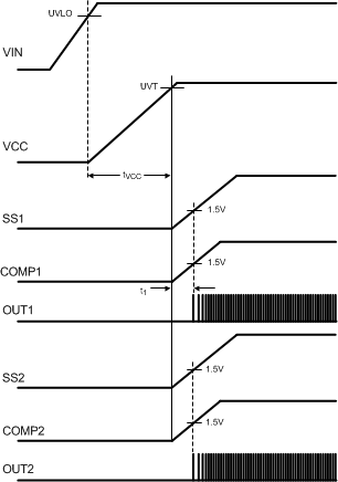 Figure 1. Startup Sequence
6.6 Typical Characteristics
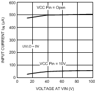 Figure 2. IIN vs VIN
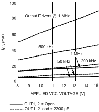 Figure 4. ICC vs Externally Applied VCC
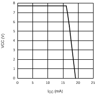 Figure 6. VCC vs ICC (Externally Loaded)
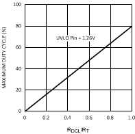 Figure 8. User Defined Maximum Duty Cycle vs RDCL Resistor
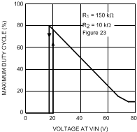 Figure 10. Maximum Duty Cycle vs. VIN (Figure 24)
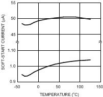 Figure 12. Soft-Start Pin Current vs Temperature
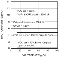 Figure 3. IIN vs VIN
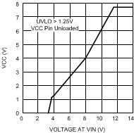 Figure 5. VCC vs VIN
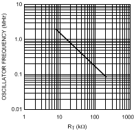 Figure 7. Oscillator Frequency vs RT Resistor
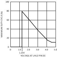 Figure 9. Maximum Duty Cycle vs. UVLO Voltage
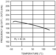 Figure 11. Frequency vs. Temperature
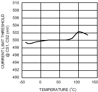 Figure 13. Current Limit Threshold at CS1, CS2 vs Temperature