SNVS703H February 2011 – November 2014 LM5046
PRODUCTION DATA.
- 1 Features
- 2 Applications
- 3 Description
- 4 Revision History
- 5 Pin Configuration and Functions
- 6 Specifications
-
7 Detailed Description
- 7.1 Overview
- 7.2 Functional Block Diagram
- 7.3
Feature Description
- 7.3.1 High-Voltage Start-Up Regulator
- 7.3.2 Line Undervoltage Detector
- 7.3.3 Overvoltage Protection
- 7.3.4 Reference
- 7.3.5 Oscillator, Sync Input
- 7.3.6 Cycle-by-Cycle Current Limit
- 7.3.7 Hiccup Mode
- 7.3.8 PWM Comparator
- 7.3.9 RAMP Pin
- 7.3.10 Slope Pin
- 7.3.11 Soft-Start
- 7.3.12 Gate Driver Outputs
- 7.3.13 Synchronous Rectifier Control Outputs (SR1 & SR2)
- 7.3.14 Soft-Start of the Synchronous Rectifiers
- 7.3.15 Pre-Bias Startup
- 7.3.16 Soft-Stop
- 7.3.17 Soft-Stop Off
- 7.3.18 Thermal Protection
- 7.4 Device Functional Modes
-
8 Application and Implementation
- 8.1 Application Information
- 8.2
Typical Application
- 8.2.1 Design Requirements
- 8.2.2
Detailed Design Procedure
- 8.2.2.1 Phase-Shifted Full-Bridge Operation
- 8.2.2.2 Control Method Selection
- 8.2.2.3 Voltage Mode Control Using the LM5046
- 8.2.2.4 Current Mode Control Using the LM5046
- 8.2.2.5 VIN and VCC
- 8.2.2.6 For Applications With > 100 V Input
- 8.2.2.7 UVLO and OVP Voltage Divider Selection
- 8.2.2.8 Current Sense
- 8.2.2.9 Hiccup Mode Current Limit Restart
- 8.2.2.10 Augmenting the Gate Drive Strength
- 8.2.3 Application Curve
- 9 Power Supply Recommendations
- 10Layout
- 11Device and Documentation Support
- 12Mechanical, Packaging, and Orderable Information
パッケージ・オプション
メカニカル・データ(パッケージ|ピン)
サーマルパッド・メカニカル・データ
- PWP|28
発注情報
8 Application and Implementation
NOTE
Information in the following applications sections is not part of the TI component specification, and TI does not warrant its accuracy or completeness. TI’s customers are responsible for determining suitability of components for their purposes. Customers should validate and test their design implementation to confirm system functionality.
8.1 Application Information
The LM5046 is a highly integrated PWM controller that contains all of the features necessary for implementing Phase Shifted Full Bridge topology power converters using either current mode or voltage mode control. The device targets DC to DC converter applications with input voltages of up to 100 Vdc and output power in the range 100W to 1kW.
8.2 Typical Application
The following schematic shows an example of a 100W phase-shifted full-bridge converter controlled by LM5046. The operating input voltage range is 36 V to 75 V, and the output voltage is 3.3 V. The output current capability is 30 Amps. The converter is configured for current mode control with external slope compensation. An auxiliary winding is used to raise the VCC voltage to reduce the controller power dissipation.
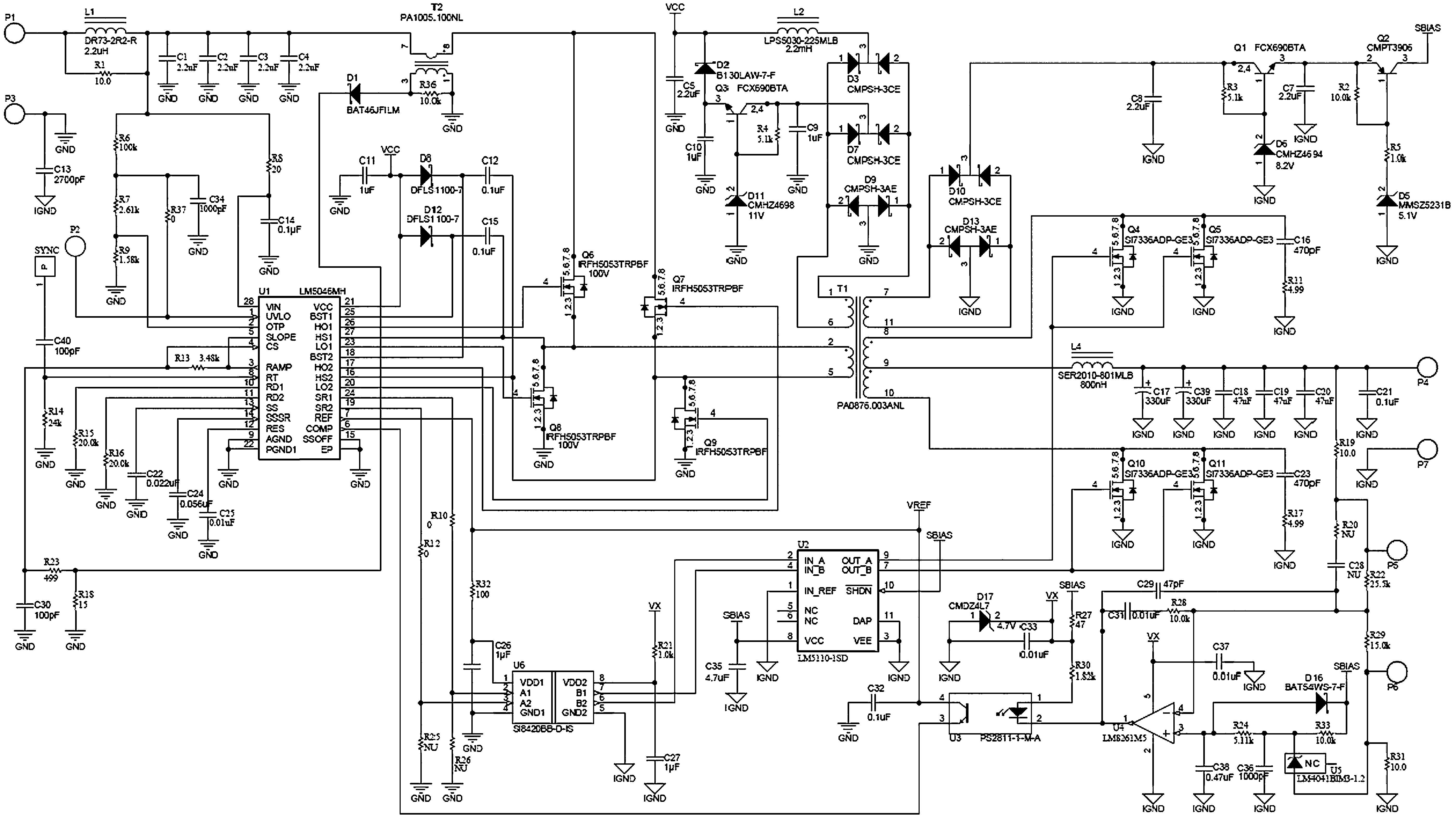
8.2.1 Design Requirements
| PARAMETERS | VALUE |
|---|---|
| Input operating range | 36 V to 75 V |
| Output voltage | 3.3 V |
| Measured efficiency at 48 V | 92% @ 30A |
| Frequency of operation | 420 kHz |
| Board size | 2.28 x 1.45 x 0.5 inches |
| Load Regulation | 0.2% |
| Line Regulation | 0.1% |
| Line UVLO | 34V/32V on/off |
| Hiccup Mode | Current Limit |
8.2.2 Detailed Design Procedure
8.2.2.1 Phase-Shifted Full-Bridge Operation
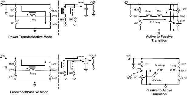 Figure 20. Operating States of the PSFB Topology
The phase shifted full-bridge topology is a derivative of the conventional full-bridge topology. When tuned appropriately the PSFB topology achieves zero voltage switching (ZVS) of the primary FETs while maintaining constant switching frequency. The ZVS feature is highly desirable as it reduces both the switching losses and the EMI emissions. The realization of the PSFB topology using the LM5046 is explained as follows:
8.2.2.1.1 Operating State 1 (Power Transfer/Active Mode)
The power transfer mode of the PSFB topology is similar to the hard switching full-bridge i.e. When the FETs in the diagonal of the bridge are turned-on (HO1 & LO2 or HO2 & LO1), a power transfer cycle from the primary to the secondary is initiated. Figure 20 depicts the case where the diagonal switches HO1 and LO2 are activated. In this state, full VIN is applied to the primary of the power transformer, which is typically stepped down on the secondary winding.
8.2.2.1.2 Operating State 2 (Active to Passive Transition)
At the end of the power transfer cycle, PWM turns off switch LO2. In the primary side, the reflected load current plus the magnetizing current propels the SW2 node towards VIN. The active to passive transition is finished when either the body diode of HO2 is forward-biased or HO2 is turned-on, whichever happens earlier. A delay can be introduced by setting RD2 to an appropriate value, such that HO2 is turned-on only after the body-diode is forward biased. In this mode, the Imag+ILpeak act as a current source charging the parasitic capacitor located at the node SW2. At light load conditions, it takes a longer time to propel SW node towards VIN.
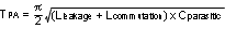
The active to passive transition time can be approximated by using Equation 6:

Where, Im is the magnetizing current, NTR is the power transformer’s turns ratio, ILpeak is the peak output filter inductor current and Cparasitic is the parasitic capacitance at the node SW2.
8.2.2.1.3 Operating State 3 (Freewheel/Passive Mode)
In the freewheel mode, unlike the conventional full-bridge topology where all the four primary FETs are off, in the PSFB topology the primary of the power transformer is shorted by activating either both the top FETs (HO1 and HO2) or both of the bottom FETs (LO1 and LO2) alternatively. In the current CLK cycle, the top FETs HO1 and HO2 are kept on together. Further in this mode, on the secondary side, similar to the classic full-bridge topology the synchronous FETs are both activated. During this state there is no energy transfer from the primary and the filter inductor current in the secondary freewheels through both the synchronous FETs.
8.2.2.1.4 Operating State 4 (Passive to Active Transition)
At the end of the switching cycle i.e. after the oscillator times out the current CLK cycle, the primary switch HO1 and the secondary FET SR1 are turned-off simultaneously. The voltage at the node SW1 begins to fall towards the GND. This is due to the resonance between leakage inductance of the power transformer plus any additional commutation inductor and the parasitic capacitances at SW1. The magnetizing inductor is shorted in the freewheel mode and therefore it does not play any role in this transition. The LC resonance results in a half-wave sinusoid whose period is determined by the leakage inductor and parasitic capacitor. The peak of the half-wave sinusoid is a function of the load current. The passive to active transition time can be approximated by using Equation 7:
When tuned appropriately either by deliberately increasing the leakage inductance or by adding an extra commutating inductor, the sinusoidal resonant waveform peaks such that it is clamped by the body-diode of the LO1 switch. At this instant, ZVS can be realized by turning on the LO1 switch.
The switching sequence in this CLK cycle is as follows: activation of the switch LO1 turns the diagonal LO1 and HO2 on, resulting in power transfer. The power transfer cycle ends when PWM turns off HO2, which is followed by an active to passive transition where LO2 is turned on. In the freewheel mode, LO1 and LO2 are both activated. From this sequence, it can be inferred that the FETs on the right side of the bridge (HO2 and LO2) are always terminated by the PWM ending a power transfer cycle and the SW2 node always sees an active to passive transition. Further, the FETs on the left side of the bridge (HO1 and LO1) are always turned-off by the CLK ending a freewheel cycle and the SW1 node always sees a passive to active transition.
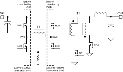 Figure 21. Simplified PSFB Topology Showing the Turn-Off Mechanism
8.2.2.2 Control Method Selection
The LM5046 is a versatile PWM control IC that can be configured for either current mode control or voltage mode control. The choice of the control method usually depends upon the designer preference. The following must be taken into consideration while selecting the control method. Current mode control can inherently balance flux in both phases of the PSFB topology. The PSFB topology, like other double ended topologies, is susceptible to the transformer core saturation. Any asymmetry in the volt-second product applied between the two alternating phases results in flux imbalance that causes a dc buildup in the transformer. This continual dc buildup may eventually push the transformer into saturation. The volt-second asymmetry can be corrected by employing current mode control. In current mode control, a signal representative of the primary current is compared against an error signal to control the duty cycle. In steady-state, this results in each phase being terminated at the same peak current by adjusting the pulse-width and thus applying equal volt-seconds to both the phases.
Current mode control can be susceptible to noise and sub-harmonic oscillation, while voltage mode control employs a larger ramp for PWM and is usually less susceptible. Voltage-mode control with input line feed-forward also has excellent line transient response. When configuring for voltage mode control, a dc blocking capacitor can be placed in series with the primary winding of the power transformer to avoid any flux imbalance that may cause transformer core saturation.
8.2.2.3 Voltage Mode Control Using the LM5046
To configure the LM5046 for voltage mode control, an external resistor (RFF) and capacitor (CFF) connected to VIN, AGND, and the RAMP pins is required to create a saw-tooth modulation ramp signal shown in Figure 22. The slope of the signal at RAMP will vary in proportion to the input line voltage. The varying slope provides line feed-forward information necessary to improve line transient response with voltage mode control. With a constant error signal, the on-time (TON) varies inversely with the input voltage (VIN) to stabilize the Volt- Second product of the transformer primary. Using a line feed-forward ramp for PWM control requires very little change in the voltage regulation loop to compensate for changes in input voltage, as compared to a fixed slope oscillator ramp. Furthermore, voltage mode control is less susceptible to noise and does not require leading edge filtering. Therefore, it is a good choice for wide input range power converters. Voltage mode control requires a Type-III compensation network, due to the complex-conjugate poles of the L-C output filter.
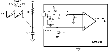 Figure 22. Feed-Forward Voltage Mode Configuration
The recommended capacitor value range for CFF is from 100 pF to 1800 pF. Referring to Figure 22, it can be seen that CFF value must be small enough to be discharged with in the clock pulse-width which is typically within 50 ns. The RDS(ON) of the internal discharge FET is 5.5 Ω.
The value of RFF required can be calculated from Equation 8.
For example, assuming a VRAMP of 1.5 V (a good compromise of signal range and noise immunity), at VINMIN of 36 V (oscillator frequency of 400 kHz and CFF = 470 pF results in a value for RFF of 125 kΩ.
8.2.2.4 Current Mode Control Using the LM5046
The LM5046 can be configured for current mode control by applying a signal proportional to the primary current to the RAMP pin. One way to achieve this is shown in Figure 23. The primary current can be sensed using a current transformer or sense resistor, the resulting signal is filtered and applied to the RAMP pin through a resistor used for slope compensation. It can be seen that the signal applied to the RAMP pin consists of the primary current information from the CS pin plus an additional ramp for slope compensation, added by the resistor RSLOPE.
The current sense resistor is selected such that during over current condition, the voltage across the current sense resistor is above the minimum CS threshold of 728 mV.
In general, the amount of slope compensation required to avoid sub-harmonic oscillation is equal to at least one-half the down-slope of the output inductor current, transformed to the primary. To mitigate sub-harmonic oscillation after one switching period, the slope compensation has to be equal to one times the down slope of the filter inductor current transposed to primary. This is known as deadbeat control. The slope compensation resistor required to implement dead-beat control can be calculated using Equation 9:
Where NTR is the turns-ratio with respect to the secondary. For example, for a 3.3 V output converter with a turns-ratio between primary and secondary of 9:1, an output filter inductance (LFILTER) of 800 nH and a current sense resistor (RSENSE) of 150 mΩ, RSLOPE of 1.67 kΩ will suffice.
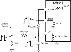 Figure 23. Current Mode Configuration
8.2.2.5 VIN and VCC
The voltage applied to the VIN pin, which may be the same as the system voltage applied to the power transformer’s primary (VPWR), can vary in the range of the 14 to 100 V. It is recommended that the filter shown in Figure 24 be used to suppress the transients that may occur at the input supply. This is particularly important when VIN is operated close to the maximum operating rating of the LM5046. The current into VIN depends primarily on the LM5046’s operating current, the switching frequency, and any external loads on the VCC pin, that typically include the gate capacitances of the power MOSFETs. In typical applications, an auxiliary transformer winding is connected through a diode to the VCC pin. This pin must raise VCC voltage above 8 V to shut off the internal start-up regulator.
After the outputs are enabled and the external VCC supply voltage has begun supplying power to the IC, the current into the VIN pin drops below 1 mA. VIN should remain at a voltage equal to or above the VCC voltage to avoid reverse current through the internal body diode of the internal VCC regulator.
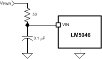 Figure 24. Input Transient Protection
8.2.2.6 For Applications With > 100 V Input
For applications where the system input voltage exceeds 100 V, VIN can be powered from an external start-up regulator as shown in Figure 25. In this configuration, the VIN and VCC pins should be connected together. The voltage at the VCC and VIN pins must be greater than 10 V (> Max VCC reference voltage) yet not exceed 16 V. To enable operation the VCC voltage must be raised above 10 V. The voltage at the VCC pin must not exceed 16 V. The voltage source at the right side of Figure 25 is typically derived from the power stage, and becomes active once the LM5046’s outputs are active.
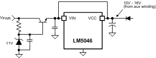 Figure 25. Start-Up Regulator for VPWR > 100 V
8.2.2.7 UVLO and OVP Voltage Divider Selection
Two dedicated comparators connected to the UVLO and OVP pins are used to detect under voltage and over voltage conditions. The threshold values of both these comparators are set at 1.25 V. The two functions can be programmed independently with two separate voltage dividers from VIN to AGND as shown in Figure 26 and Figure 27, or with a three-resistor divider as shown in Figure 28. Independent UVLO and OVP pins provide greater flexibility for the user to select the operational voltage range of the system. When the UVLO pin voltage is below 0.4 V, the controller is in a low current shutdown mode. For a UVLO pin voltage greater than 0.4 V but less than 1.25 V the controller is in standby mode. Once the UVLO pin voltage is greater than 1.25 V, the controller is fully enabled. Two external resistors can be used to program the minimum operational voltage for the power converter as shown in Figure 26. When the UVLO pin voltage falls below the 1.25 V threshold, an internal 20 µA current sink is enabled to lower the voltage at the UVLO pin, thus providing threshold hysteresis. Resistance values for R1 and R2 can be determined from Equation 10:
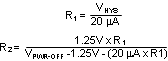
Where VPWR is the desired turn-on voltage and VHYS is the desired UVLO hysteresis at VPWR.
For example, if the LM5046 is to be enabled when VPWR reaches 33 V, and disabled when VPWR is decreased to 31 V, R1 should be 100 kΩ, and R2 should be 4.2 kΩ. The voltage at the UVLO pin should not exceed 7 V at any time.
Two external resistors can be used to program the maximum operational voltage for the power converter as shown in Figure 27. When the OVP pin voltage rises above the 1.25 V threshold, an internal 20 µA current source is enabled to raise the voltage at the OVP pin, thus providing threshold hysteresis. Resistance values for R1 and R2 can be determined from Equation 11:
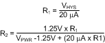
If the LM5046 is to be disabled when VPWR-OFF reaches 80 V and enabled when it is decreased to 78 V. R1 should be 100 kΩ, and R2 should be 1.5 kΩ. The voltage at the OVP pin should not exceed 7 V at any time.
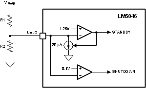 Figure 26. Basic UVLO Configuration
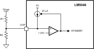 Figure 27. Basic OVP Configuration
The UVLO and OVP can also be set together using a 3 resistor divider ladder as shown in Figure 28. R1 is calculated as explained in the basic UVLO divider selection. Using the same values, as in the above two examples, for the UVLO and OVP set points, R1 and R3 remain the same at 100 kΩ and 1.5 kΩ. The R2 is 2.7 kΩ obtained by subtracting R3 from 4.2 kΩ.
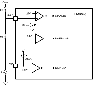 Figure 28. UVLO/OVP Divider
Remote configuration of the controller’s operational modes can be accomplished with open drain device(s) connected to the UVLO pin as shown in Figure 29.
Figure 30 shows an application of the OVP comparator for Remote Thermal Protection using a thermistor (or multiple thermistors) which may be located near the main heat sources of the power converter. The negative temperature coefficient (NTC) thermistor is nearly logarithmic, and in this example a 100 kΩ thermistor with the β material constant of 4500 Kelvin changes to approximately 2 kΩ at 130ºC. Setting R1 to one-third of this resistance (665 Ω) establishes 130ºC as the desired trip point (for VREF = 5 V). In a temperature band from 20ºC below to 20ºC above the OVP threshold, the voltage divider is nearly linear with 25mV per ºC sensitivity.
R2 provides temperature hysteresis by raising the OVP comparator input by R2 x 20 µA. For example, if a 22 kΩ resistor is selected for R2, then the OVP pin voltage will increase by 22k x 20 µA = 506 mV. The NTC temperature must therefore fall by 506 mV / 25 mV per ºC = 20ºC before the LM5046 switches from standby mode to the normal mode.
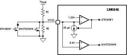 Figure 29. Remote Standby and Disable Control
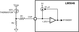 Figure 30. Remote Thermal Protection
8.2.2.8 Current Sense
The CS pin receives an input signal representative of its transformer’s primary current, either from a current sense transformer or from a resistor located at the junction of source pin of the primary switches, as shown in Figure 31 and Figure 32, respectively. In both the cases, the filter components RF and CF should be located as close to the IC as possible, and the ground connection from the current sense transformer, or RSENSE should be a dedicated trace to the appropriate GND pin. Please refer to the layout section for more layout tips.
The current sense components must provide a signal > 710 mV at the CS pin during an over-load event. Once the voltage on the CS pin crosses the current limit threshold, the current sense comparator terminates the PWM pulse and starts to charge the RES pin. Depending on the configuration of the RES pin, the LM5046 will eventually initiate a hiccup mode restart or be in continuous current limit.
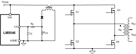 Figure 31. Transformer Current Sense
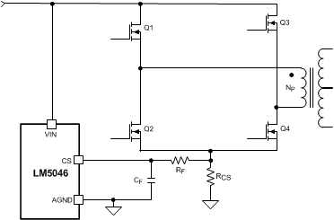 Figure 32. Resistor Current Sense
8.2.2.9 Hiccup Mode Current Limit Restart
The operation of the hiccup mode restart circuit is explained in the Overview section. During a continuous current limit condition, the RES pin is charged with 30 µA current source. The restart delay time required to reach the 1.0 V threshold is given by Equation 12:

This establishes the number of current limit events allowed before the IC initiates a hiccup restart sequence. For example, if the CRES = 0.01 µF, the time TCS as noted in Figure 33 is 334 µs. Once the RES pin reaches 1.0 V, the 30 µA current source is turned-off and a 10 µA current source is turned-on during the ramp up to 4 V and a 5 µA is turned on during the ramp down to 2 V. The hiccup mode off-time is given by Equation 13:

With a CRES= 0.01 µF, the hiccup time is 49 ms. Once the hiccup time is finished, the RES pin is pulled-low and the SS pin is released allowing a soft-start sequence to commence. Once the SS pin reaches 1 V, the PWM pulses will commence. The hiccup mode provides a cool-down period for the power converter in the event of a sustained overload condition thereby lowering the average input current and temperature of the power components during such an event.
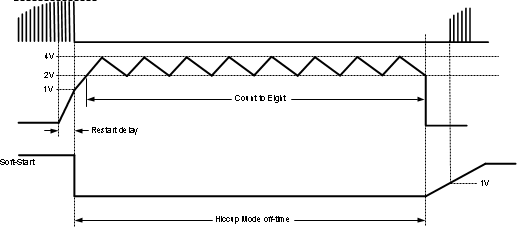 Figure 33. Hiccup Mode Delay and Soft-Start Timing Diagram
8.2.2.10 Augmenting the Gate Drive Strength
The LM5046 includes powerful 2A integrated gate drivers. However, in certain high power applications (> 500W), it might be necessary to augment the strength of the internal gate driver to achieve higher efficiency and better thermal performance. In high power applications, typically, the I2xR loss in the primary MOSFETs is significantly higher than the switching loss. In order to minimize the I2xR loss, either the primary MOSFETs are paralleled or MOSFETs with low RDS (on) are employed. Both these scenarios increase the total gate charge to be driven by the controller IC. An increase in the gate charge increases the FET transition time and hence increases the switching losses. Therefore, to keep the total losses within a manageable limit the transition time needs to be reduced.
Generally, during the miller capacitance charge/discharge the total available driver current is lower during the turn-off process than during the turn-on process and often it is enough to speed-up the turn-off time to achieve the efficiency and thermal goals. This can be achieved simply by employing a PNP device, as shown in Figure 34, from gate to source of the power FET. During the turn-on process, when the LO1 goes high, the current is sourced through the diode D1 and the BJT Q1 provides the path for the turn-off current. Q1 should be located as close to the power FET as possible so that the turn-off current has the shortest possible path to the ground and does not have to pass through the controller.
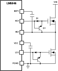 Figure 34. Circuit to Speed-up the Turn-off Process
Depending on the gate charge characteristics of the primary FET, if it is required to speed up both the turn-on and the turn-off time, a bipolar totem pole structure as shown in Figure 35 can be used. When LO1 goes high, the gate to source current is sourced through the NPN transistor Q1 and similar to the circuit shown in Figure 34 when LO1 goes low the PNP transistor Q2 expedites the turn-off process.
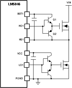 Figure 35. Bipolar Totem Pole Arrangement
Alternatively, a low side gate driver such as LM5112 can be utilized instead of the discrete totem pole. The LM5112 comes in a small package with a 3A source and a 7A sink capability. While driving the high-side FET, the HS1 acts as a local ground and the boot capacitor between the BST and HS pins acts as VCC.
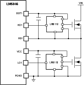 Figure 36. Using a Low Side Gate Driver to Augment Gate Drive Strength
8.2.3 Application Curve
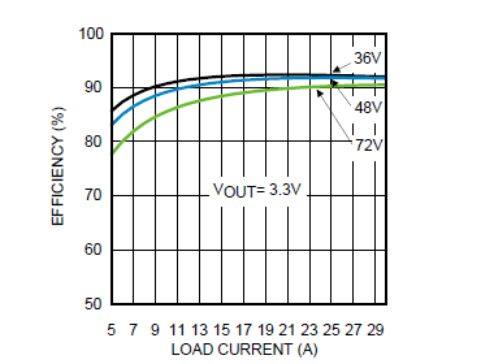 Figure 37. Application Board Efficiency