JAJSGX1G September   2006  – Jaunuary 2020 LM5069

PRODUCTION DATA.  

  1. 特長
  2. アプリケーション
  3. 概要
    1.     Device Images
      1.      代表的なアプリケーションの図
  4. 改訂履歴
    1.     Device Comparison
  5. Pin Configuration and Functions
    1.     Pin Functions
  6. Specifications
    1. 6.1 Absolute Maximum Ratings
    2. 6.2 ESD Ratings
    3. 6.3 Recommended Operating Conditions
    4. 6.4 Thermal Information
    5. 6.5 Electrical Characteristics
    6. 6.6 Typical Characteristics
  7. Detailed Description
    1. 7.1 Overview
    2. 7.2 Functional Block Diagram
    3. 7.3 Feature Description
      1. 7.3.1 Current Limit
      2. 7.3.2 Circuit Breaker
      3. 7.3.3 Power Limit
      4. 7.3.4 Undervoltage Lockout (UVLO)
      5. 7.3.5 Overvoltage Lockout (OVLO)
      6. 7.3.6 Power Good Pin
    4. 7.4 Device Functional Modes
      1. 7.4.1 Power Up Sequence
      2. 7.4.2 Gate Control
      3. 7.4.3 Fault Timer and Restart
      4. 7.4.4 Shutdown Control
  8. Application and Implementation
    1. 8.1 Application Information
    2. 8.2 Typical Application
      1. 8.2.1 48-V, 10-A Hot Swap Design
        1. 8.2.1.1 Design Requirements
        2. 8.2.1.2 Detailed Design Procedure
          1. 8.2.1.2.1 Select RSNS and CL setting
          2. 8.2.1.2.2 Selecting the Hot Swap FET(s)
          3. 8.2.1.2.3 Select Power Limit
          4. 8.2.1.2.4 Set Fault Timer
          5. 8.2.1.2.5 Check MOSFET SOA
          6. 8.2.1.2.6 Set Undervoltage and Overvoltage Threshold
            1. 8.2.1.2.6.1 Option A
            2. 8.2.1.2.6.2 Option B
            3. 8.2.1.2.6.3 Option C
            4. 8.2.1.2.6.4 Option D
          7. 8.2.1.2.7 Input and Output Protection
          8. 8.2.1.2.8 Final Schematic and Component Values
        3. 8.2.1.3 Application Curves
  9. Power Supply Recommendations
  10. 10Layout
    1. 10.1 Layout Guidelines
      1. 10.1.1 PC Board Guidelines
      2. 10.1.2 System Considerations
    2. 10.2 Layout Example
  11. 11デバイスおよびドキュメントのサポート
    1. 11.1 デバイス・サポート
      1. 11.1.1 開発サポート
    2. 11.2 ドキュメントのサポート
      1. 11.2.1 関連資料
    3. 11.3 ドキュメントの更新通知を受け取る方法
    4. 11.4 コミュニティ・リソース
    5. 11.5 商標
    6. 11.6 静電気放電に関する注意事項
    7. 11.7 Glossary
  12. 12メカニカル、パッケージ、および注文情報

パッケージ・オプション

メカニカル・データ(パッケージ|ピン)
サーマルパッド・メカニカル・データ
発注情報

Power Good Pin

During turnon, the Power Good pin (PGD) is high until the voltage at VIN increases above ≊ 5 V. PGD then switches low, remaining low as the VIN voltage increases. When the voltage at OUT increases to within 1.25 V of the SENSE pin (VDS <1.25 V), PGD switches high. PGD switches low if the VDS of Q1 increases above 2.5 V. A pullup resistor is required at PGD as shown in Figure 20. The pullup voltage (VPGD) can be as high as 80 V, with transient capability to 100 V, and can be higher or lower than the voltages at VIN and OUT.
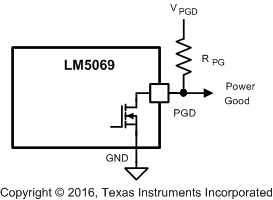
LM5069 20197251.gifFigure 20. Power Good Output

If a delay is required at PGD, suggested circuits are shown in Figure 21. In Figure 21a, capacitor CPG adds delay to the rising edge, but not to the falling edge. In Figure 21b, the rising edge is delayed by RPG1 + RPG2 and CPG, while the falling edge is delayed a lesser amount by RPG2 and CPG. Adding a diode across RPG2 (Figure 21c) allows for equal delays at the two edges, or a short delay at the rising edge and a long delay at the falling edge.
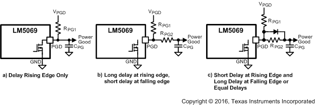
LM5069 20197252.gifFigure 21. Adding Delay to the Power Good Output Pin