JAJSRS8I February 2007 – November 2023 LM5116
PRODUCTION DATA
- 1
- 1 特長
- 2 アプリケーション
- 3 概要
- 4 Pin Configuration and Functions
- 5 Specifications
- 6 Detailed Description
-
7 Application and Implementation
- 7.1 Application Information
- 7.2
Typical Application
- 7.2.1 Design Requirements
- 7.2.2
Detailed Design Procedure
- 7.2.2.1 Custom Design with WEBENCH® Tools
- 7.2.2.2 Timing Resistor
- 7.2.2.3 Output Inductor
- 7.2.2.4 Current Sense Resistor
- 7.2.2.5 Ramp Capacitor
- 7.2.2.6 Output Capacitors
- 7.2.2.7 Input Capacitors
- 7.2.2.8 VCC Capacitor
- 7.2.2.9 Bootstrap Capacitor
- 7.2.2.10 Soft Start Capacitor
- 7.2.2.11 Output Voltage Divider
- 7.2.2.12 UVLO Divider
- 7.2.2.13 MOSFETs
- 7.2.2.14 MOSFET Snubber
- 7.2.2.15 Error Amplifier Compensation
- 7.2.2.16 Comprehensive Equations
- 7.2.3 Application Curves
- 7.3 Power Supply Recommendations
- 7.4 Layout
- 8 Device and Documentation Support
- 9 Revision History
- 10Mechanical, Packaging, and Orderable Information
5.7 Typical Performance Characteristics
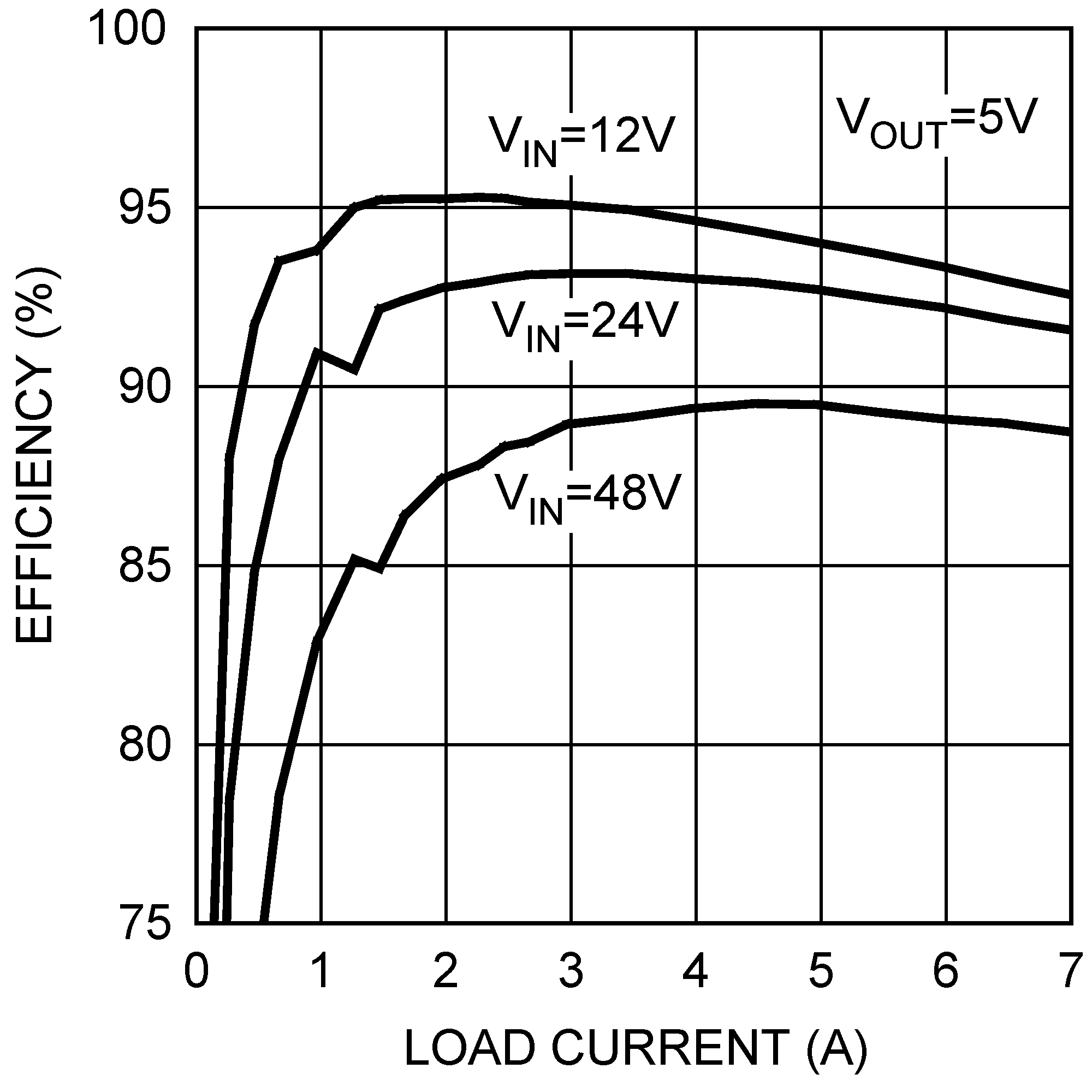 Figure 5-1 Typical Application Circuit
Efficiency
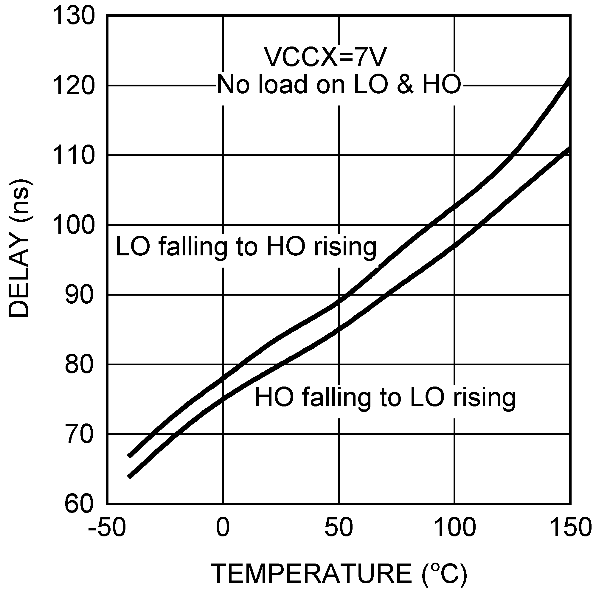 Figure 5-3 Driver Dead-time vs
Temperature
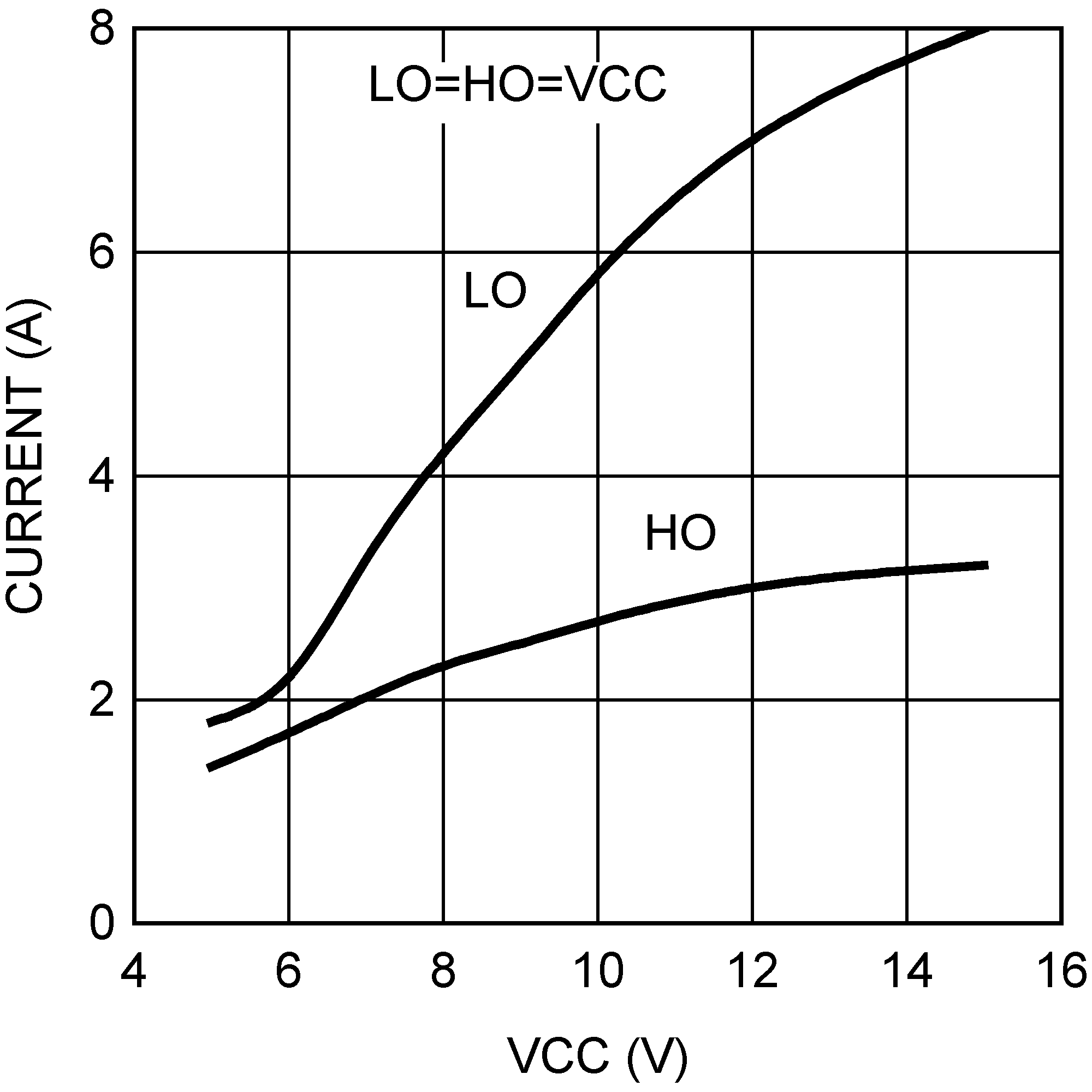 Figure 5-5 Driver Sink Current vs VCC
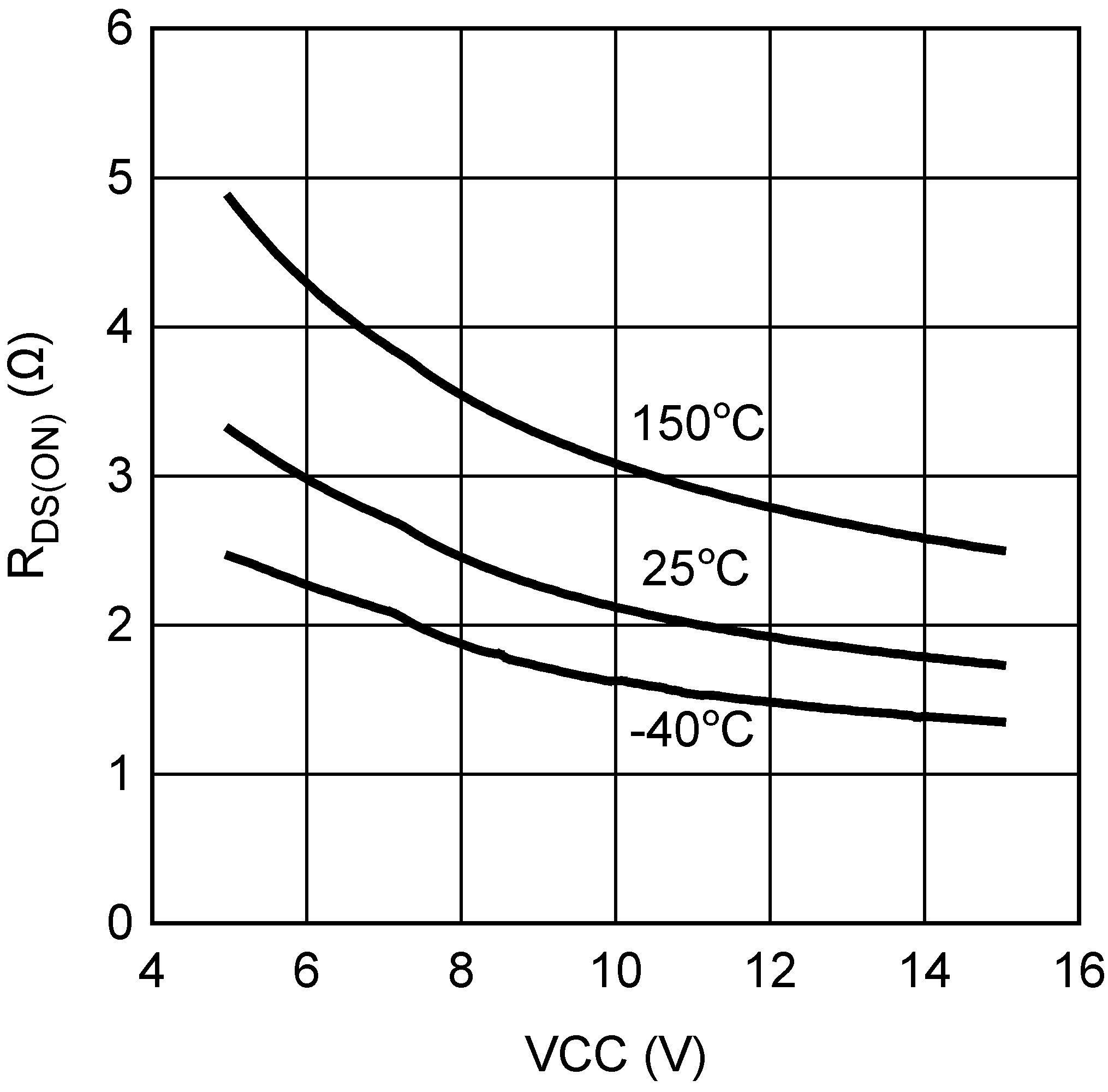 Figure 5-7 LO High RDS(ON) vs
VCC
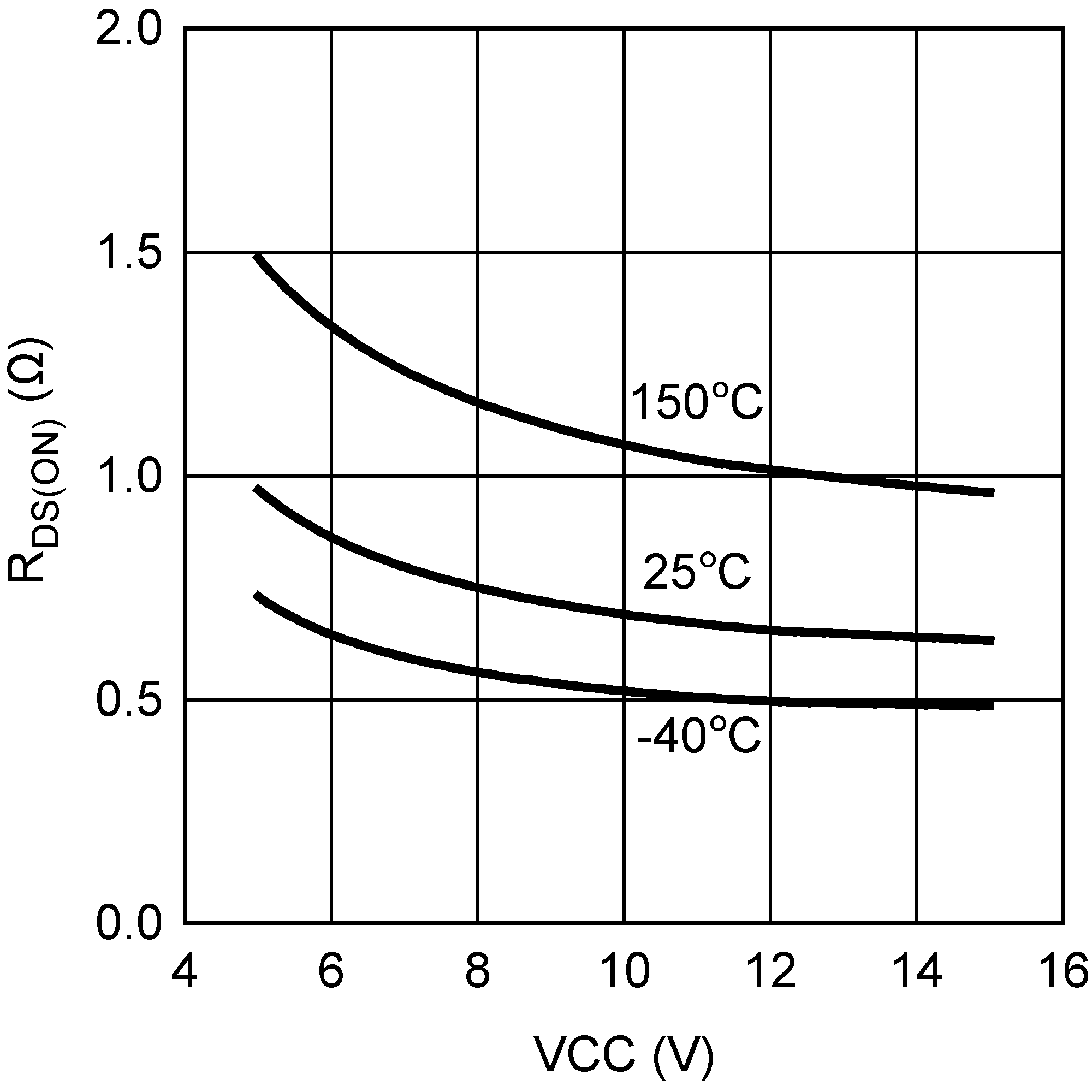 Figure 5-9 LO Low RDS(ON) vs
VCC
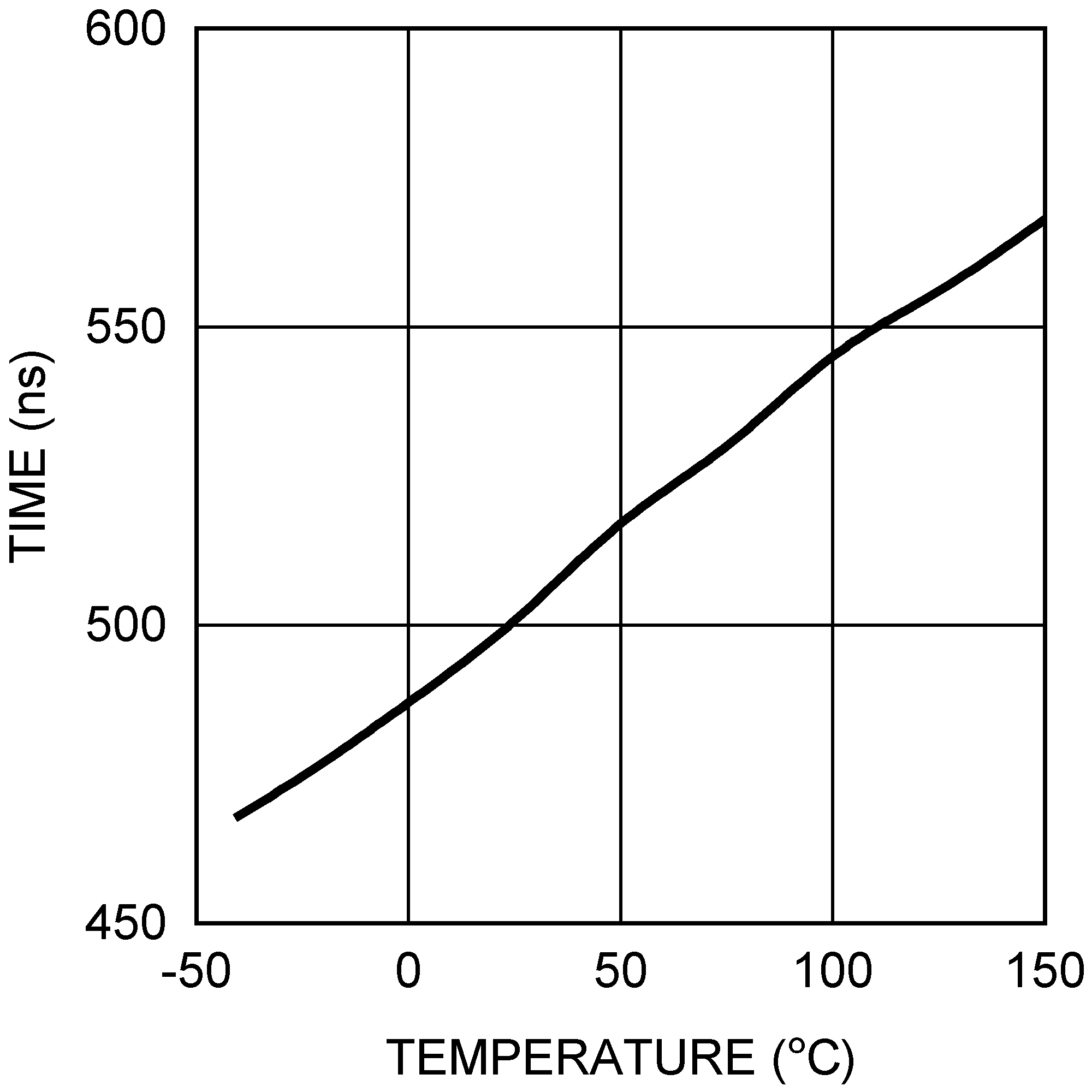 Figure 5-11 Forced HO Off-time vs Temperature
VCCX = 5 V
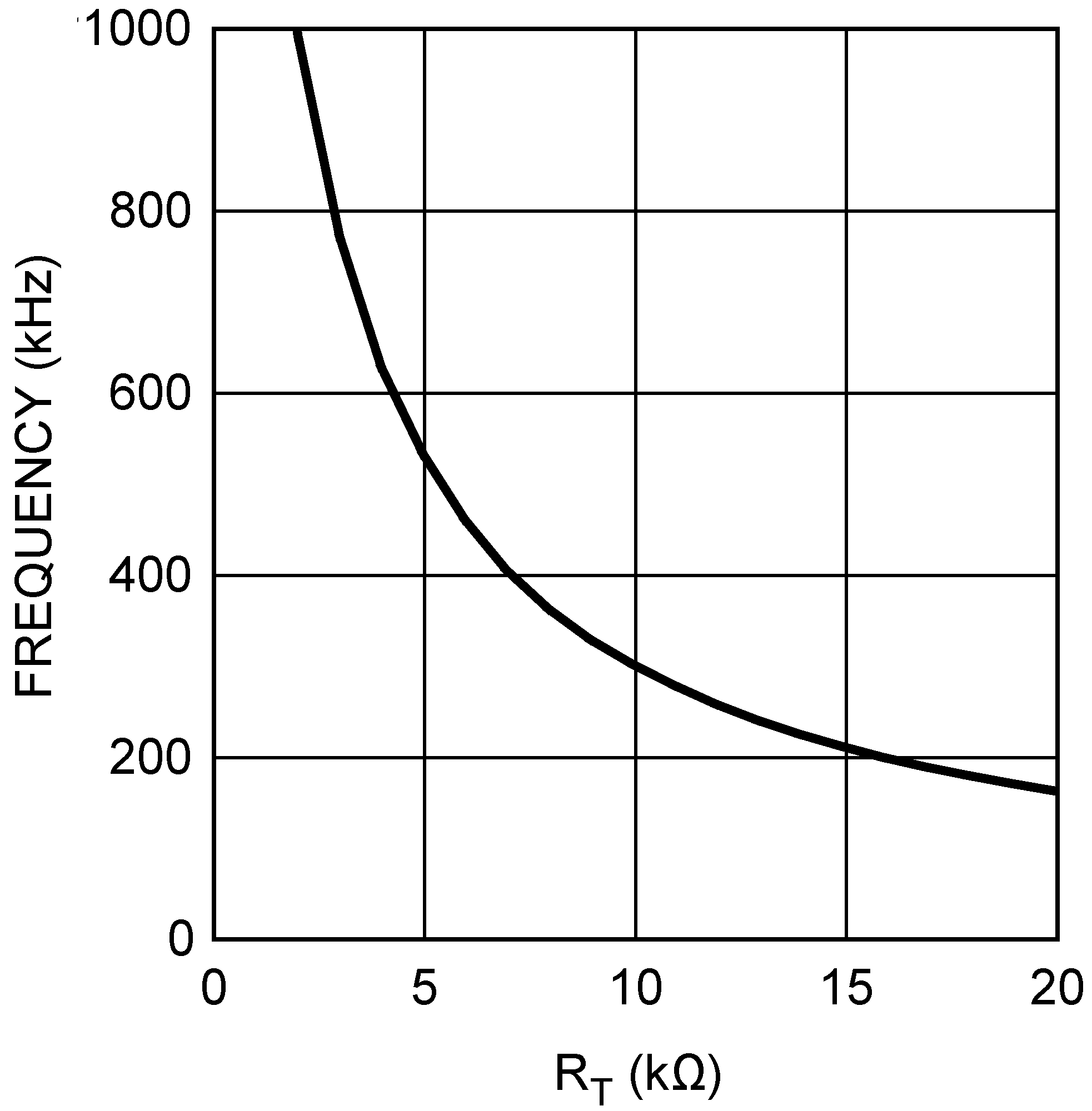 Figure 5-13 Frequency vs RT
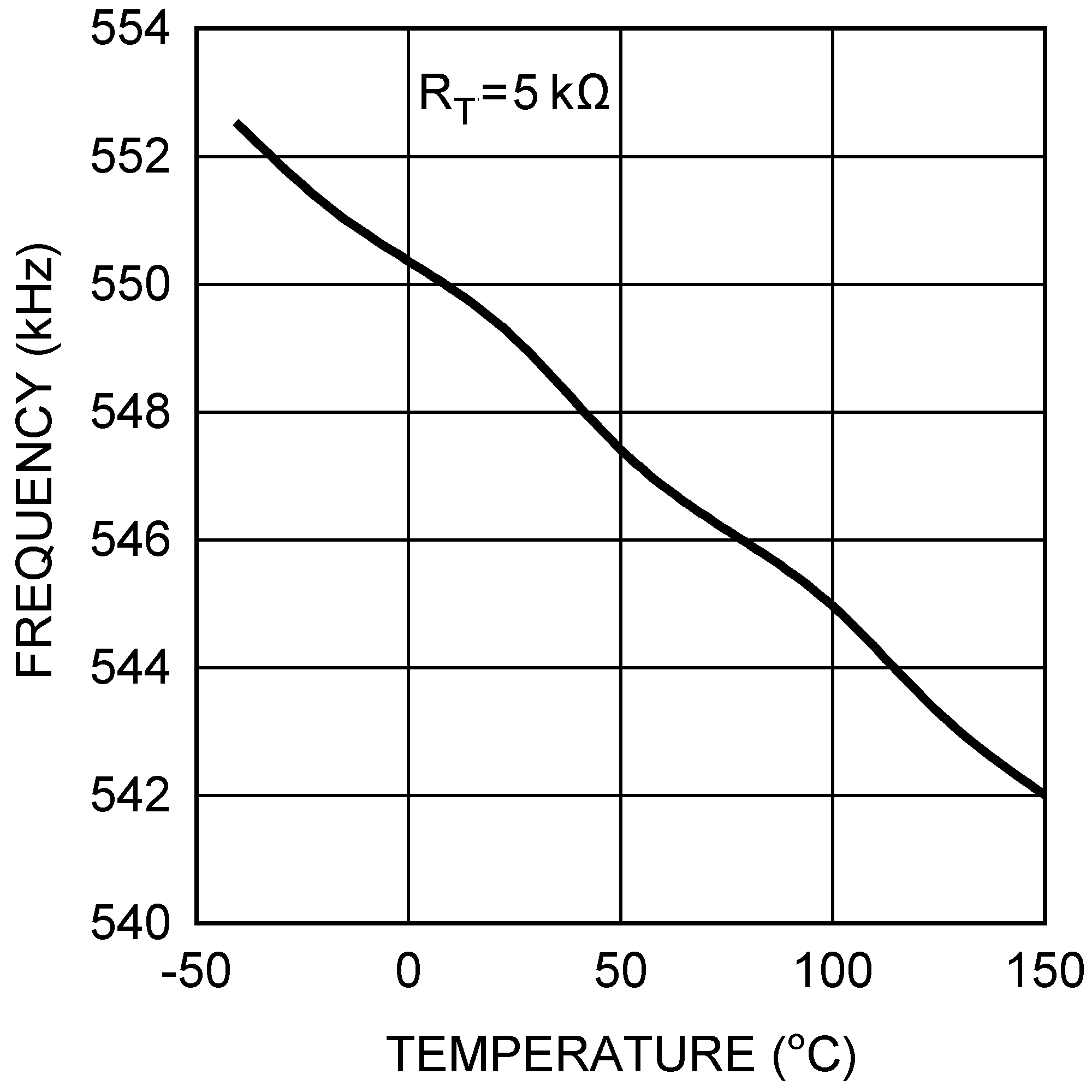 Figure 5-15 Frequency vs Temperature
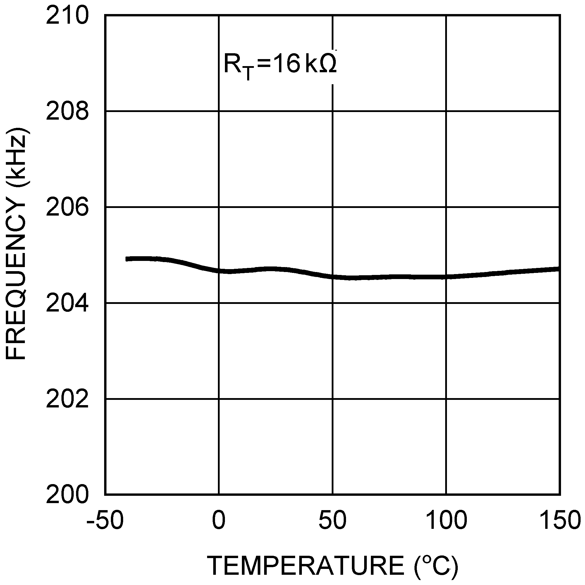 Figure 5-17 Frequency vs Temperature
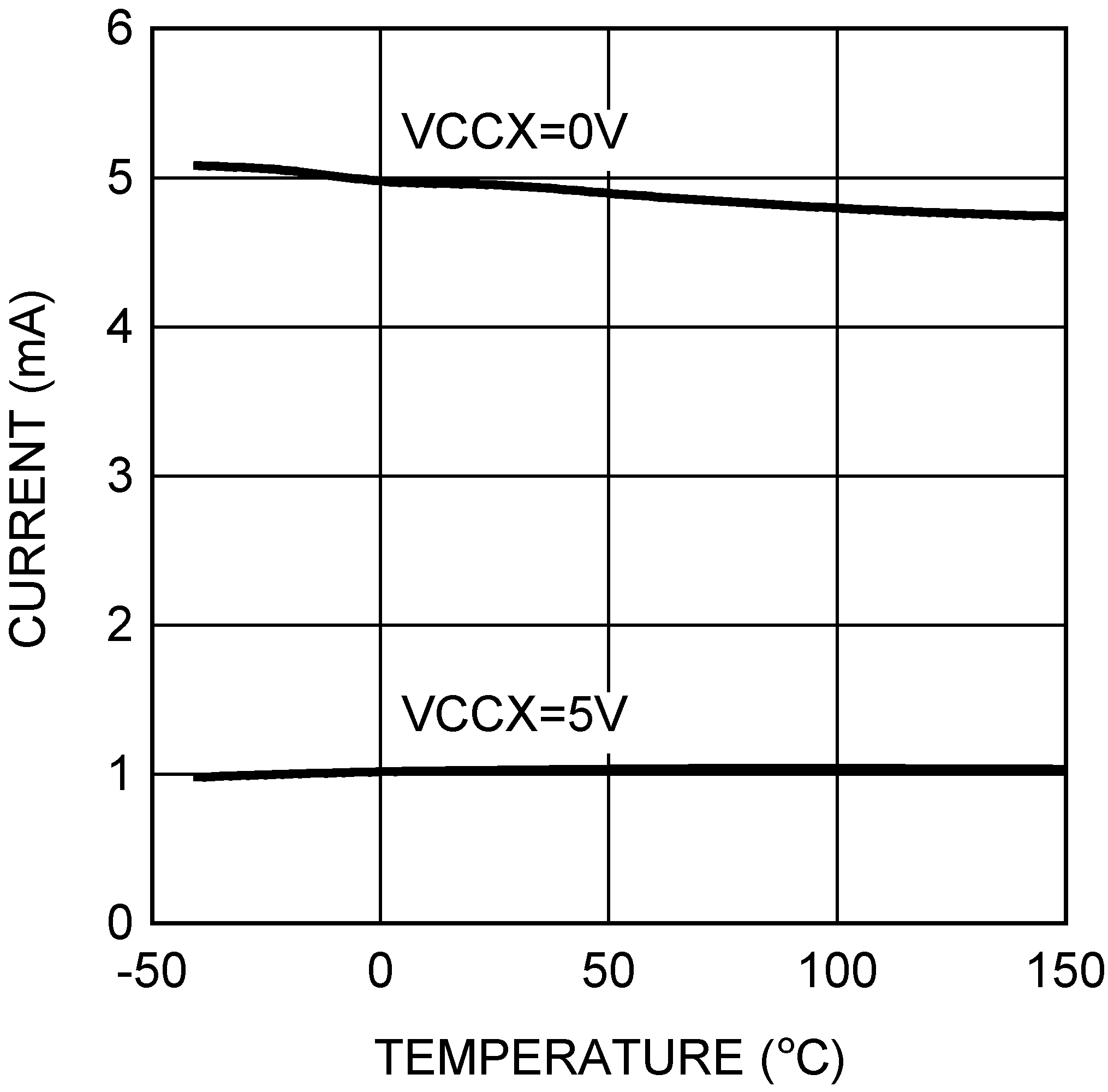 Figure 5-19 VIN Operating Current vs
Temperature
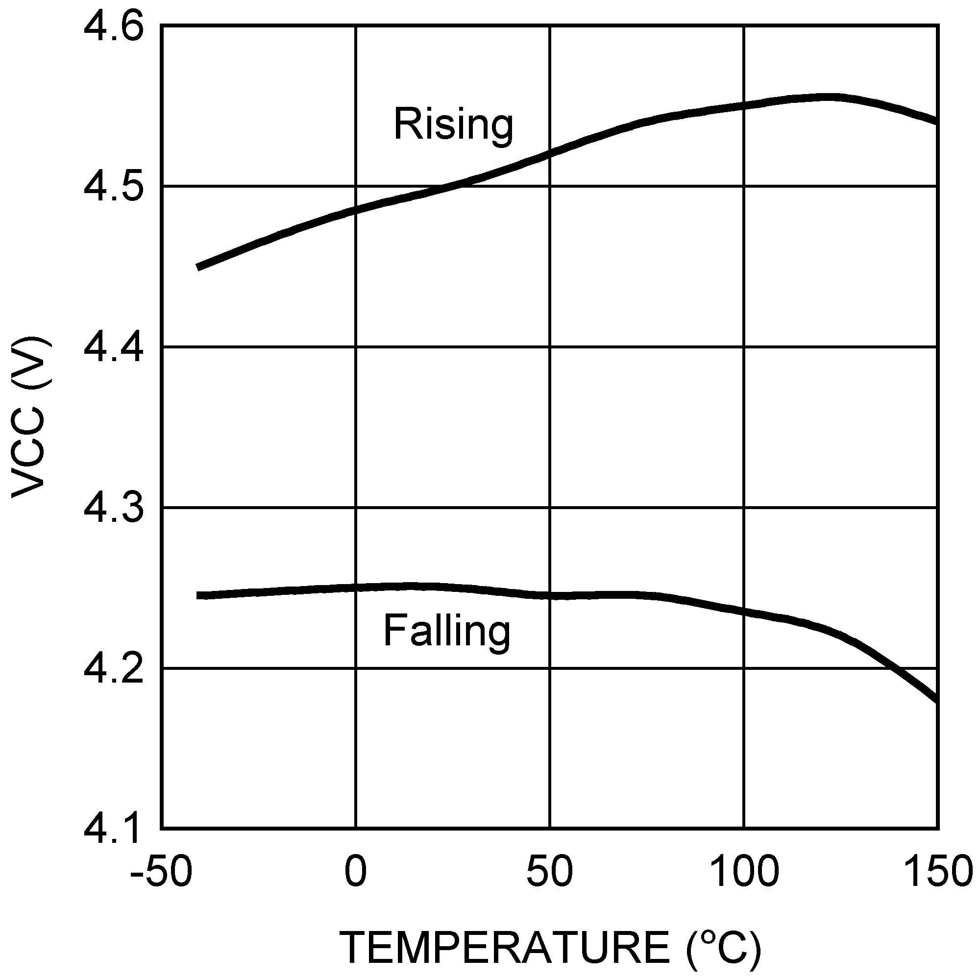 Figure 5-21 VCC UVLO vs Temperature
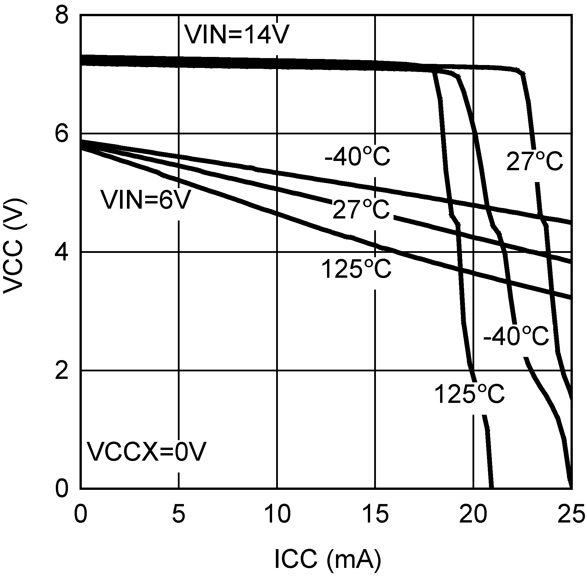 Figure 5-23 VCC vs ICC
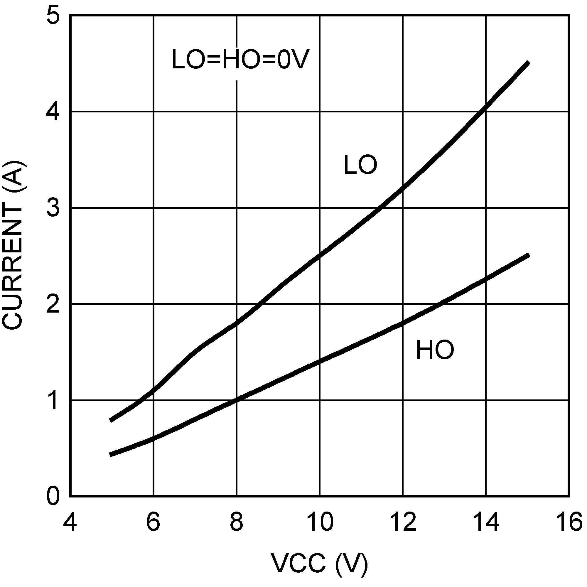 Figure 5-2 Driver Source Current vs
VCC
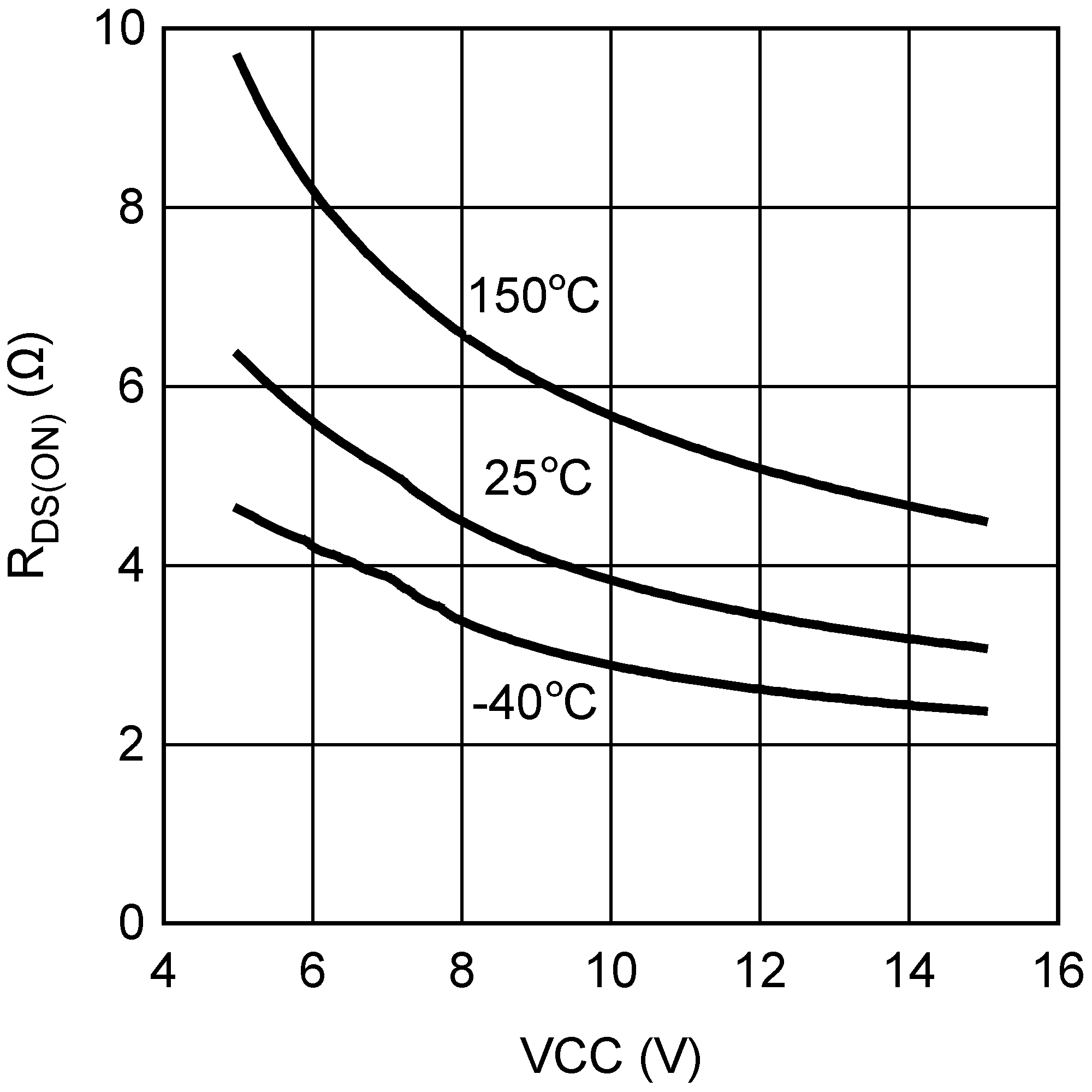 Figure 5-4 HO High RDS(ON) vs
VCC
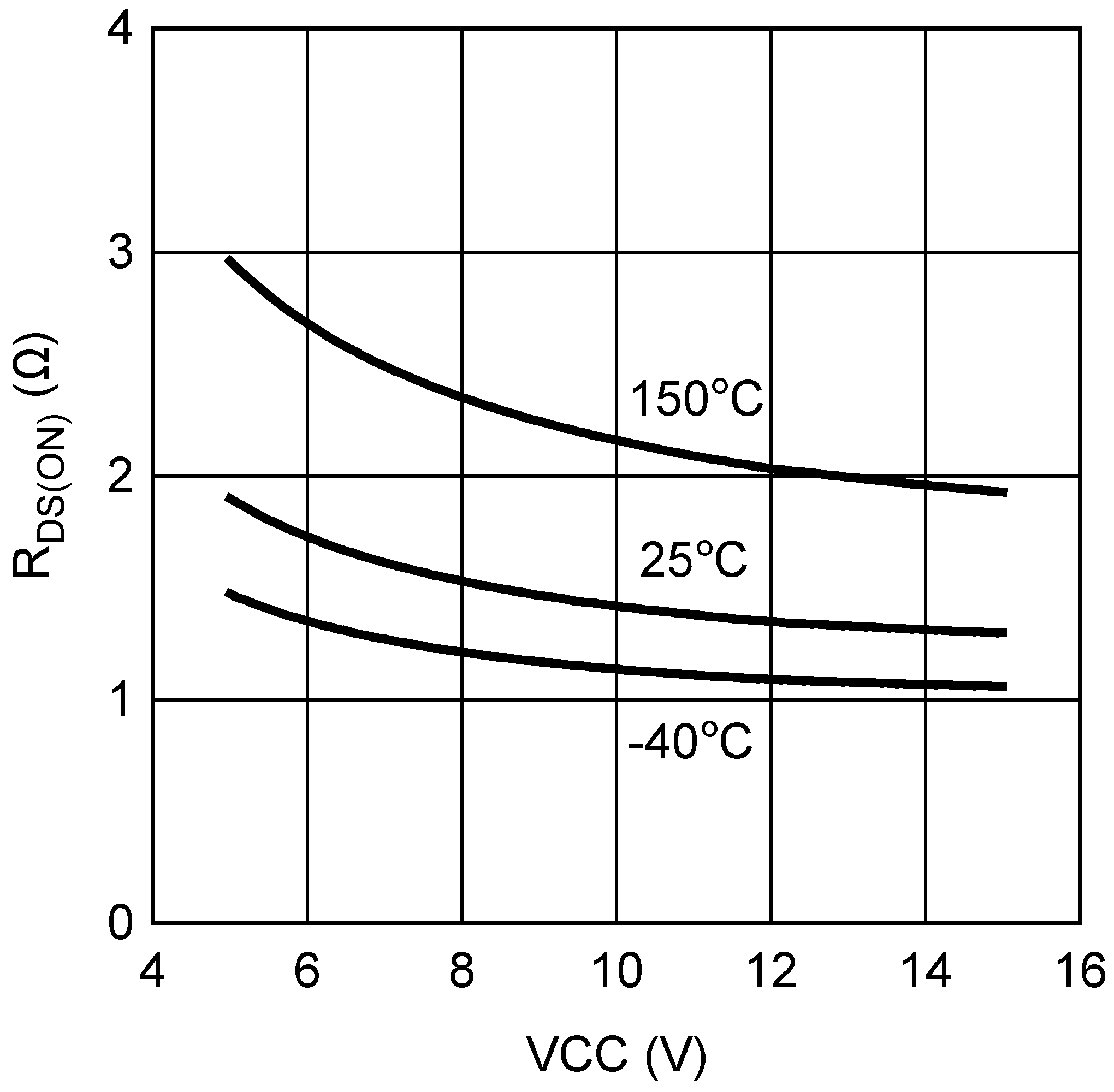 Figure 5-6 HO Low RDS(ON) vs
VCC
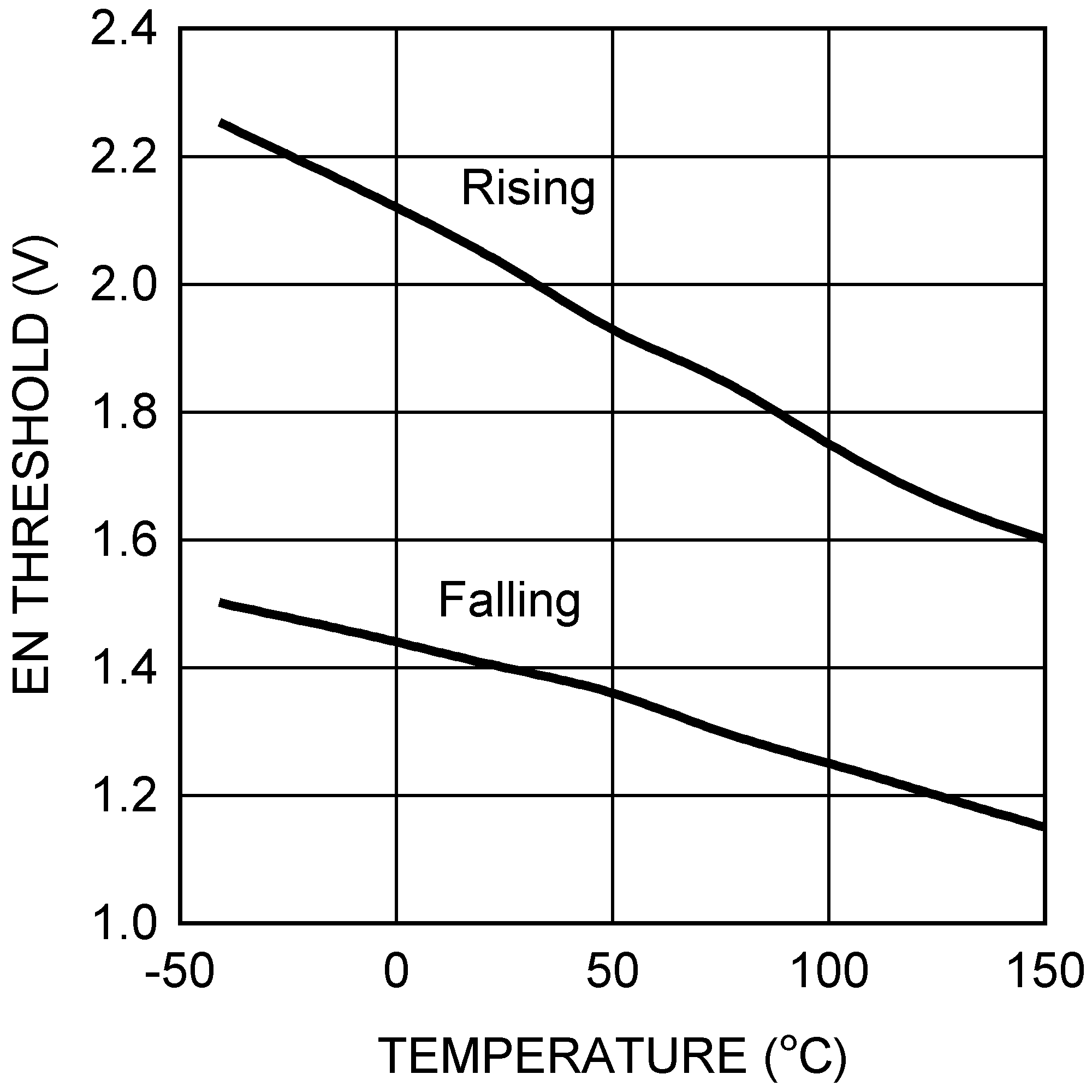 Figure 5-8 EN Input Threshold vs
Temperature
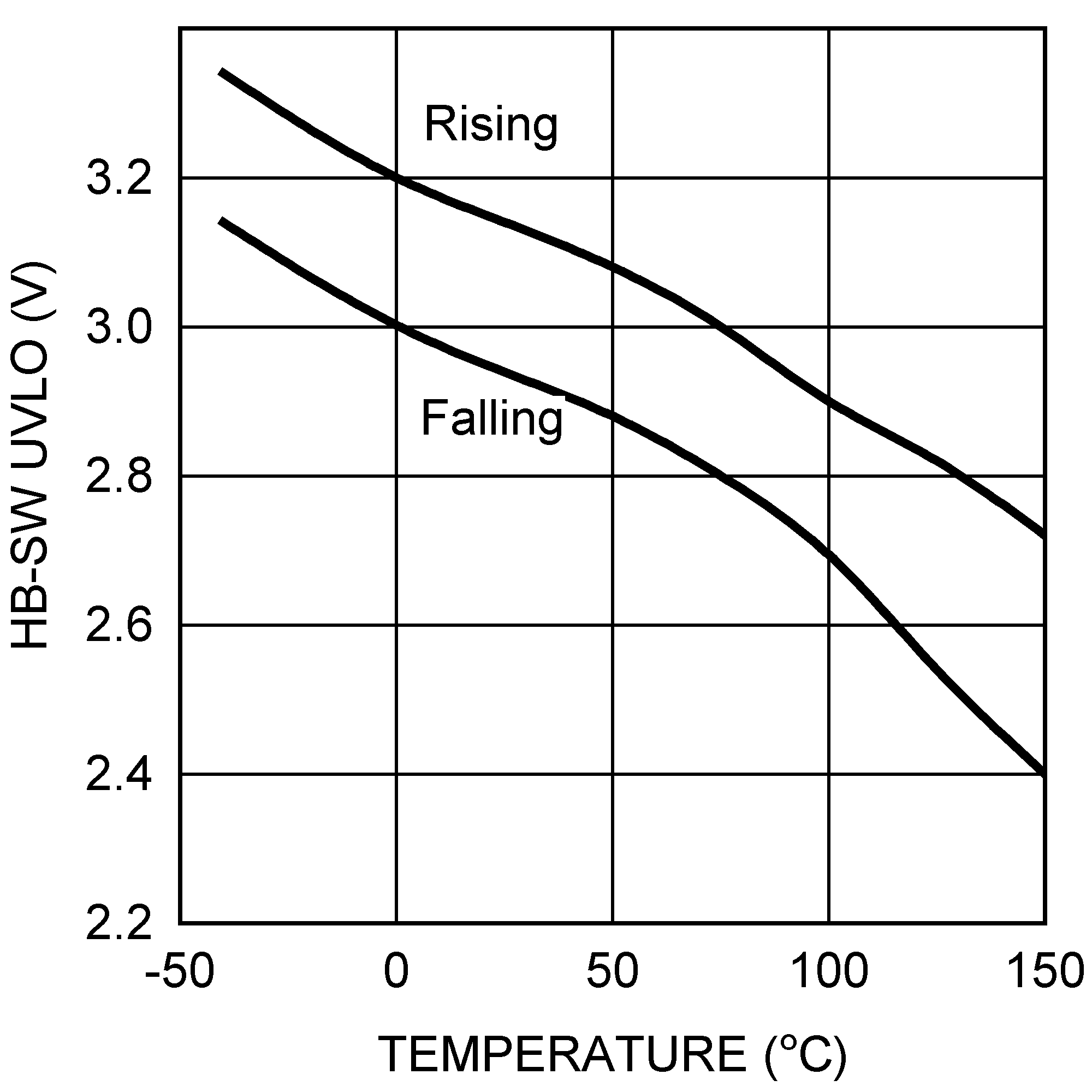 Figure 5-10 HB to SW UVLO vs
Temperature
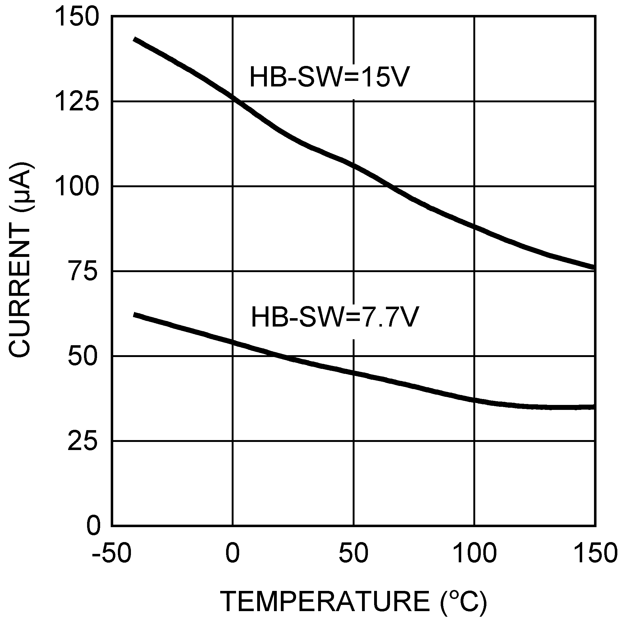 Figure 5-12 HB DC Bias Current vs
Temperature
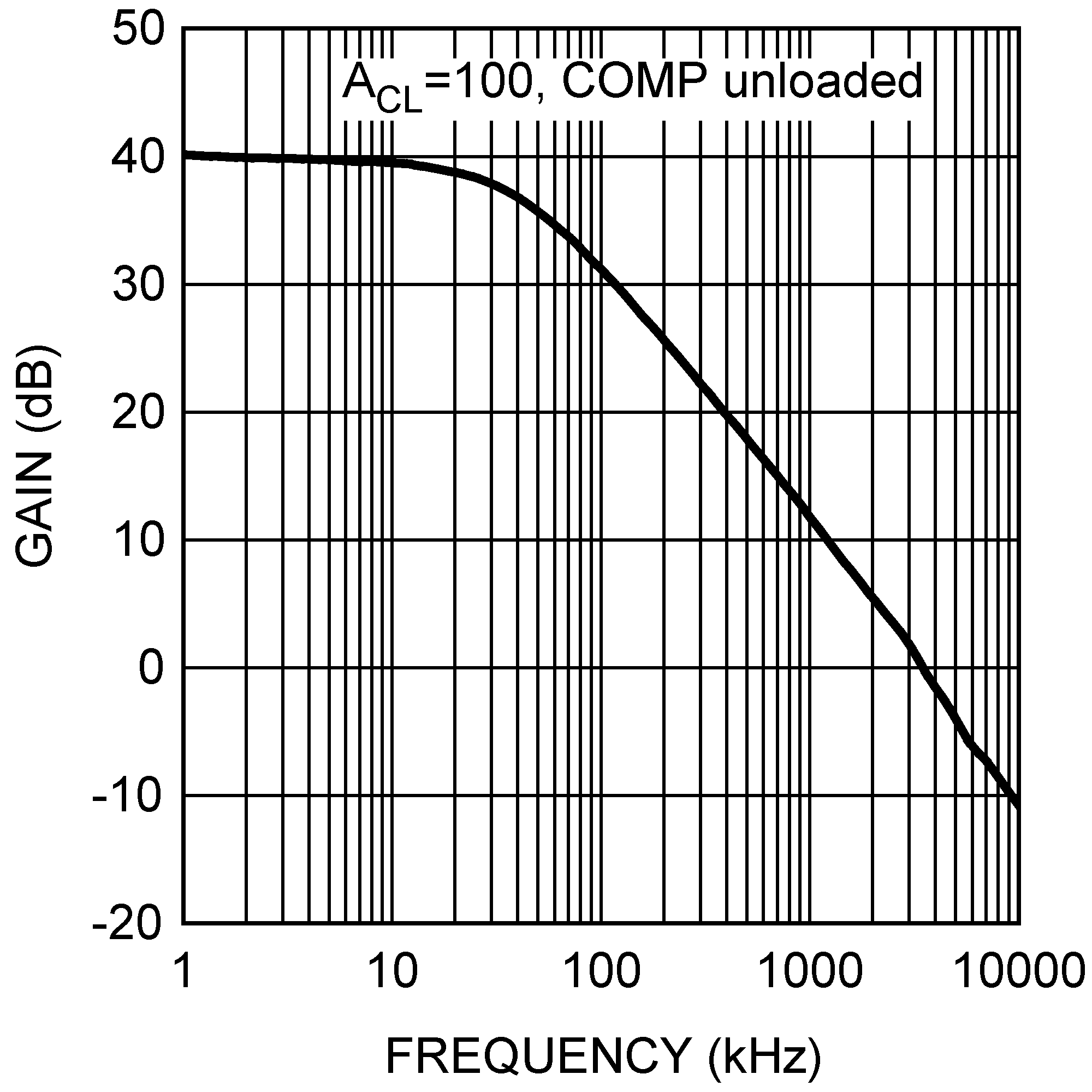 Figure 5-14 Error Amp Gain vs Frequency
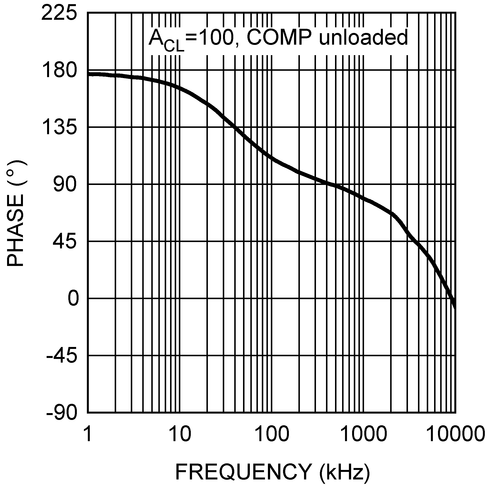 Figure 5-16 Error Amp Phase vs
Frequency
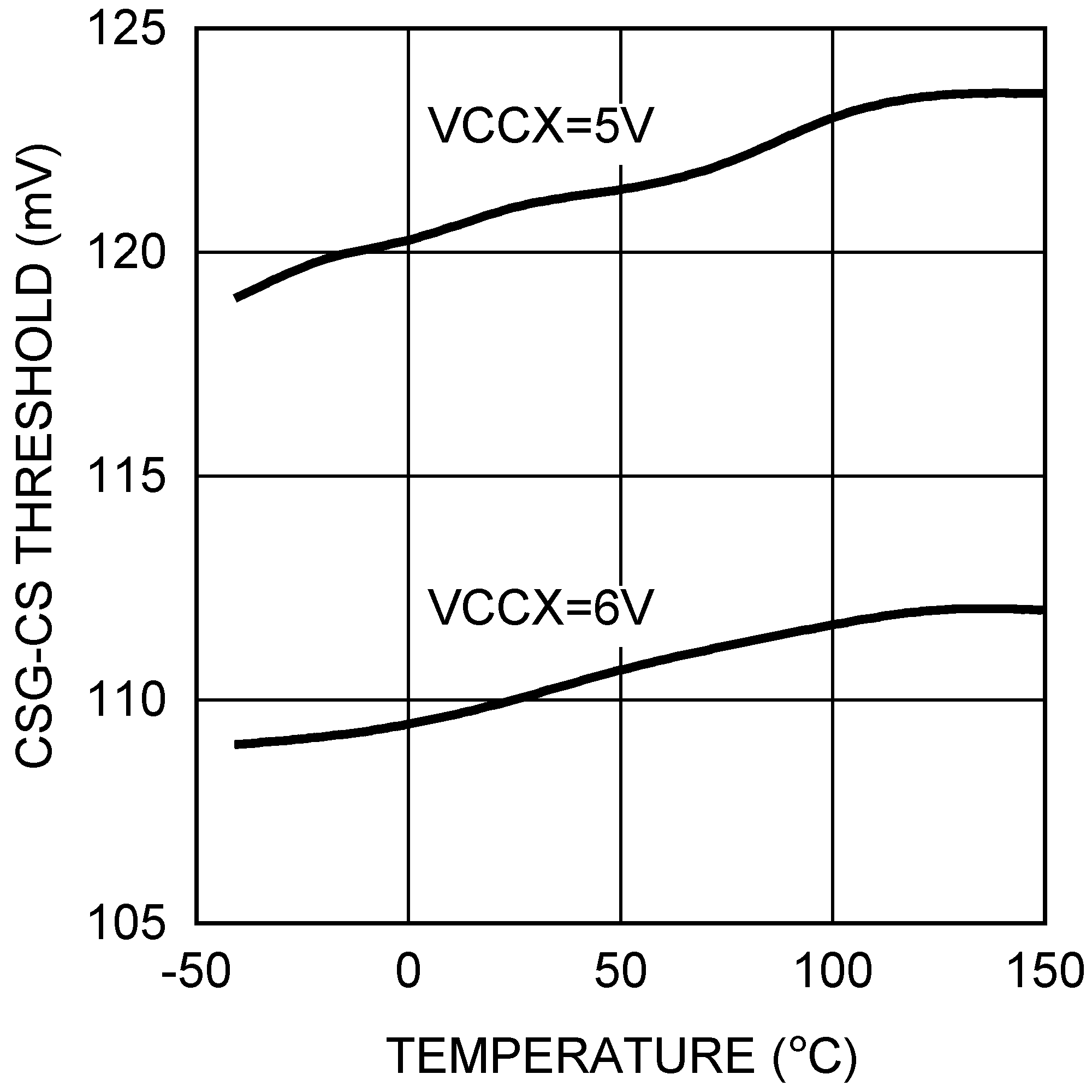 Figure 5-18 Current Limit Threshold vs
Temperature
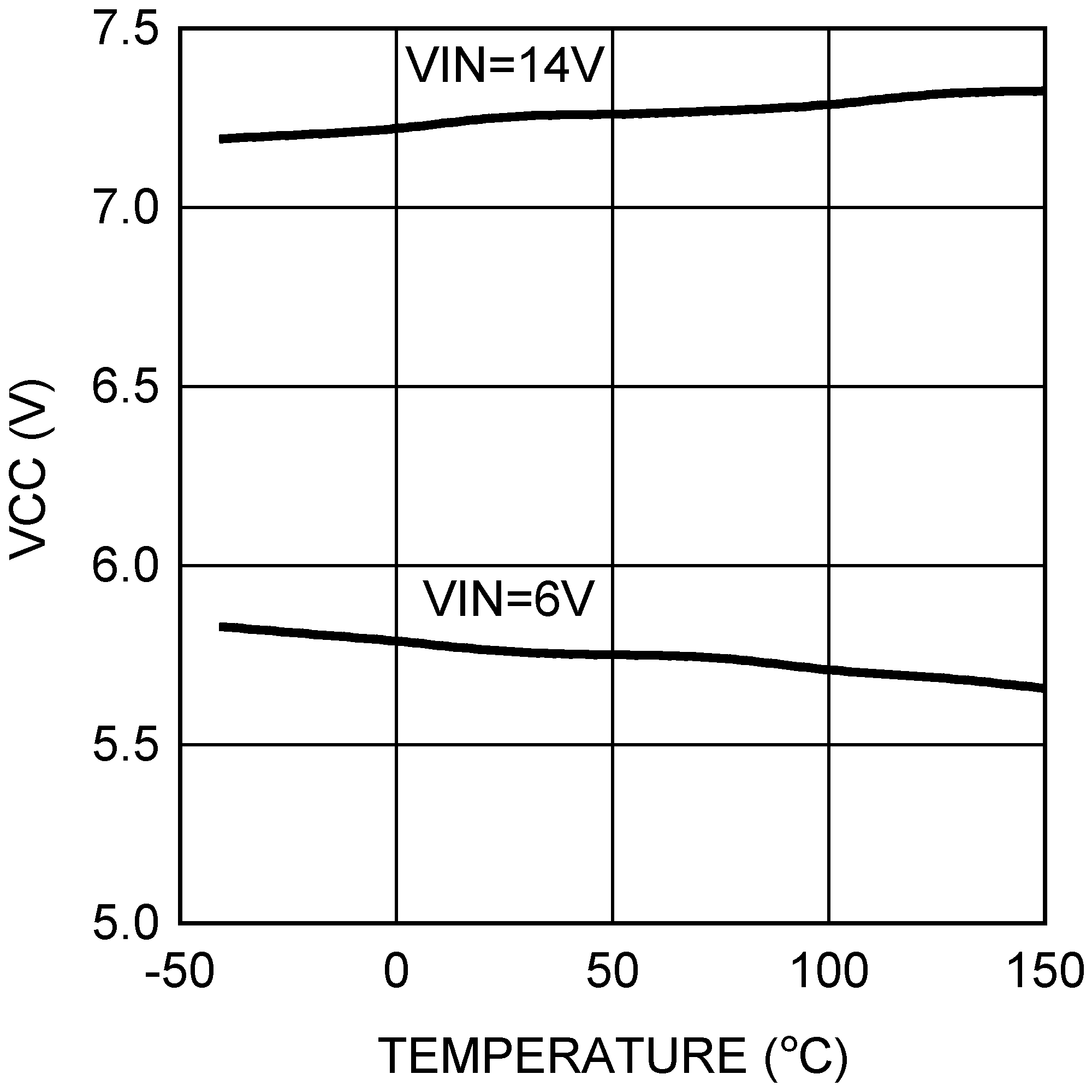 Figure 5-20 VCC vs Temperature
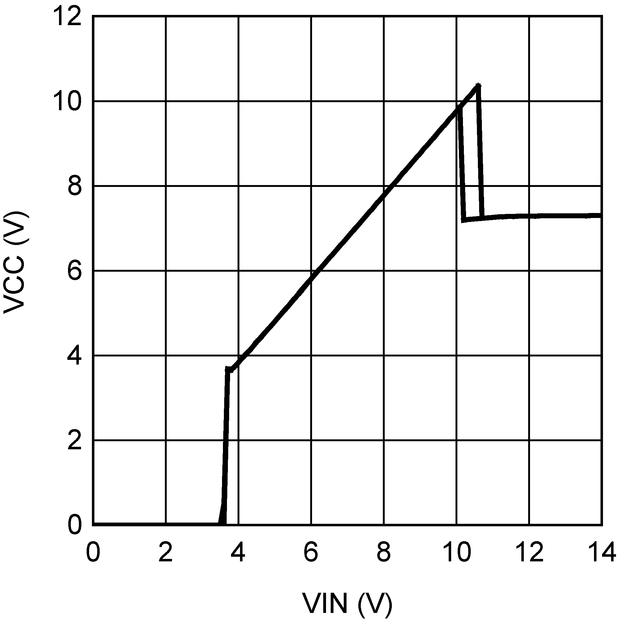 Figure 5-22 VCC vs VIN
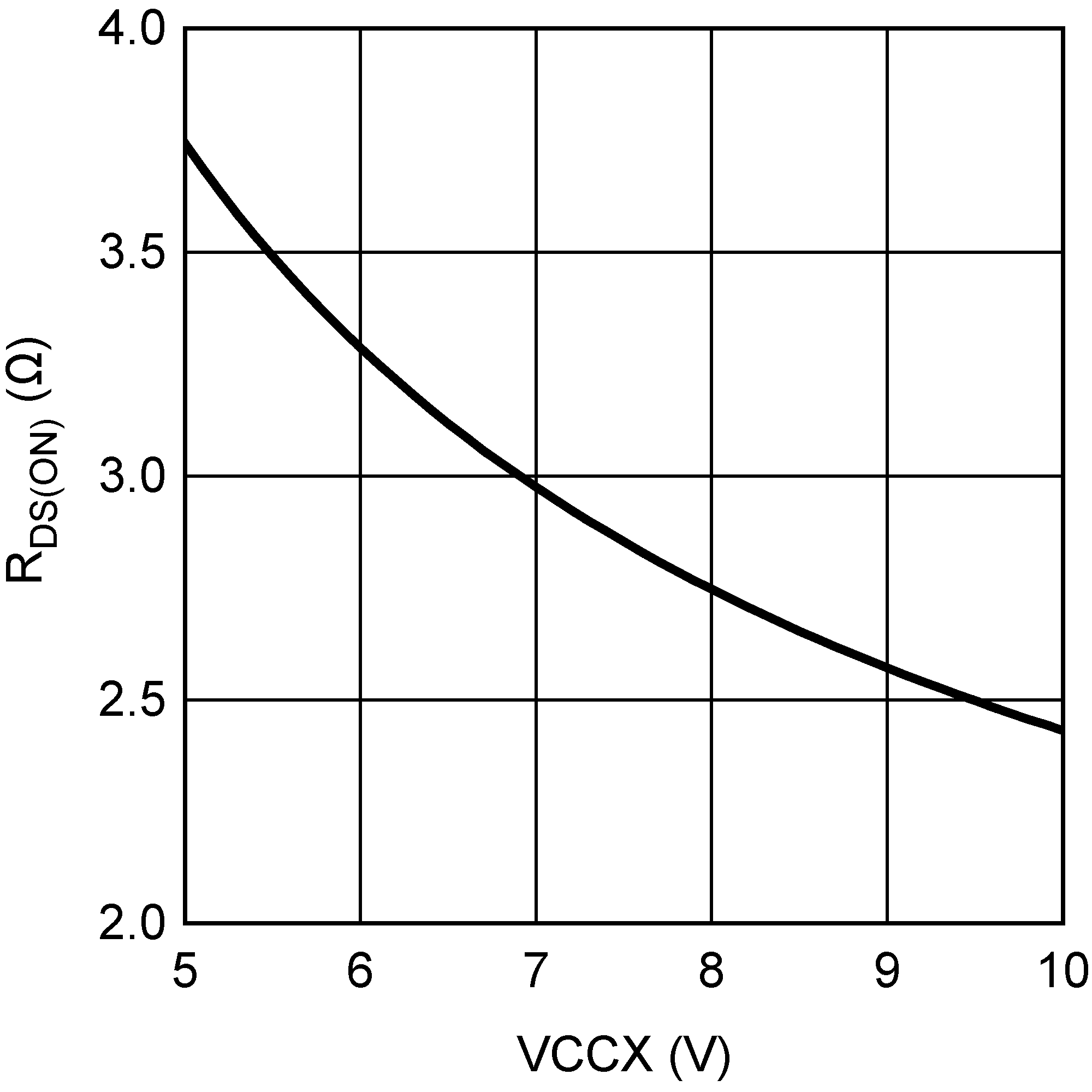 Figure 5-24 VCCX Switch RDS(ON) vs
VCCX