JAJSDX2C September 2017 – October 2021 LM5150-Q1
PRODUCTION DATA
- 1 特長
- 2 アプリケーション
- 3 概要
- 4 Revision History
- 5 Device Comparison Table
- 6 Pin Configuration and Functions
- 7 Specifications
-
8 Detailed Description
- 8.1 Overview
- 8.2 Functional Block Diagram
- 8.3
Feature Description
- 8.3.1 Enable (EN Pin)
- 8.3.2 High Voltage VCC Regulator (PVCC, AVCC Pin)
- 8.3.3 Power-On Voltage Selection (VSET Pin)
- 8.3.4 Switching Frequency (RT Pin)
- 8.3.5 Clock Synchronization (SYNC Pin in SS Configuration)
- 8.3.6 Current Sense, Slope Compensation, and PWM (CS Pin)
- 8.3.7 Current Limit (CS Pin)
- 8.3.8 Feedback and Error Amplifier (COMP Pin)
- 8.3.9 Automatic Wake-Up and Standby
- 8.3.10 Boost Status Indicator (STATUS Pin)
- 8.3.11 Maximum Duty Cycle Limit, Minimum Input Supply Voltage
- 8.3.12 MOSFET Driver (LO Pin)
- 8.3.13 Thermal Shutdown
- 8.4 Device Functional Modes
-
9 Application and Implementation
- 9.1 Application Information
- 9.2
Typical Application
- 9.2.1 Design Requirements
- 9.2.2
Detailed Design Procedure
- 9.2.2.1 Custom Design With WEBENCH® Tools
- 9.2.2.2 RSET Resistor
- 9.2.2.3 RT Resistor
- 9.2.2.4 Inductor Selection (LM)
- 9.2.2.5 Current Sense (RS)
- 9.2.2.6 Slope Compensation Ramp (RSL)
- 9.2.2.7 Output Capacitor (COUT)
- 9.2.2.8 Loop Compensation Component Selection and Maximum ESR
- 9.2.2.9 PVCC Capacitor, AVCC Capacitor, and AVCC Resistor
- 9.2.2.10 VOUT Filter (CVOUT, RVOUT)
- 9.2.2.11 Input Capacitor
- 9.2.2.12 MOSFET Selection
- 9.2.2.13 Diode Selection
- 9.2.2.14 Efficiency Estimation
- 9.2.3 Application Curves
- 9.3 System Examples
- 10Power Supply Recommendations
- 11Layout
- 12Device and Documentation Support
- 13Mechanical, Packaging, and Orderable Information
パッケージ・オプション
デバイスごとのパッケージ図は、PDF版データシートをご参照ください。
メカニカル・データ(パッケージ|ピン)
- RUM|16
サーマルパッド・メカニカル・データ
発注情報
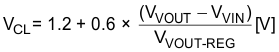
8.3.7 Current Limit (CS Pin)
The LM5150-Q1 features cycle-by-cycle peak current limit without subharmonic oscillation at high duty cycle. If the sum of the sensed inductor current and the slope compensation ramp exceeds the current limit threshold at the current limit comparator input (VCL), the current limit comparator immediately terminates the present cycle. To minimize the peak current limit variation due to changes in either the supply voltage or the output voltage, the device features a variable current limit threshold which is calculated using Equation 6.
Cycle-by-cycle peak inductor current limit (IPEAK-CL) in steady state calculated as follows:
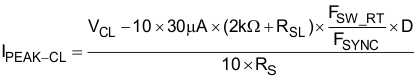
FSYNC is included in the equation because the peak amplitude of the slope compensation varies with the frequency of the external synchronization clock. Substitute FSW_RT for FSYNC if clock synchronization is not used.
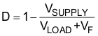
Boost converters have a natural pass-through path from the supply to the load through the high-side power diode (D1). Due to this path, boost converters cannot provide current limit protection when the output voltage is close to or less than the input supply voltage.
A small external RC filter (RF, CF) at the CS pin is required to overcome the leading edge spike of the current sense signal. Select an RF value which is greater than 30 Ω and a CF value which is greater than 1 nF. Due to the effect of the filter, the peak current limit is not valid when the on-time is less than 2 × RF × CF.