JAJSGZ0A March 2019 – September 2019 LM76202-Q1
PRODUCTION DATA.
- 1 特長
- 2 アプリケーション
- 3 概要
- 4 改訂履歴
- 5 Pin Configuration and Functions
- 6 Specifications
- 7 Parameter Measurement Information
-
8 Detailed Description
- 8.1 Overview
- 8.2 Functional Block Diagram
- 8.3
Feature Description
- 8.3.1 Undervoltage Lockout (UVLO)
- 8.3.2 Overvoltage Protection (OVP)
- 8.3.3 Reverse Battery Protection
- 8.3.4 Hot Plug-In and In-Rush Current Control
- 8.3.5 Overload and Short Circuit Protection
- 8.4 Device Functional Modes
-
9 Application and Implementation
- 9.1 Application Information
- 9.2
Typical Application
- 9.2.1 Design Requirements
- 9.2.2 Detailed Design Procedure
- 9.2.3 Application Curves
- 10Power Supply Recommendations
- 11Layout
- 12デバイスおよびドキュメントのサポート
- 13メカニカル、パッケージ、および注文情報
パッケージ・オプション
デバイスごとのパッケージ図は、PDF版データシートをご参照ください。
メカニカル・データ(パッケージ|ピン)
- PWP|16
サーマルパッド・メカニカル・データ
発注情報
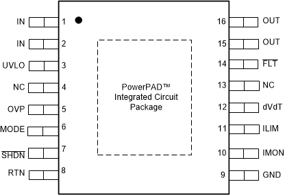
5 Pin Configuration and Functions
PWP Package
16-Pin HTSSOP With Exposed Thermal Pad
Top View

Pin Functions
| PIN | TYPE | DESCRIPTION | |
|---|---|---|---|
| NO. | NAME | ||
| 1, 2 | IN | P | Input supply voltage. See IN, OUT, RTN and GND Pins section. |
| 3 | UVLO | I | Input for setting the programmable Undervoltage Lockout threshold. An undervoltage event turns off the internal FET and asserts FLT to indicate power failure. If the Undervoltage Lockout function is not needed, the UVLO terminal must be connected to the IN terminal. See Undervoltage Lockout (UVLO) section. |
| 4, 13 | NC | — | No internal connection. These pins can be connected to RTN for enhanced thermal performance. |
| 5 | OVP | I | Input for setting the programmable Overvoltage Protection threshold. An overvoltage event turns off the internal FET and asserts FLT to indicate the overvoltage fault. For fixed overvoltage clamp response connect OVP to RTN externally. See Overvoltage Protection (OVP) section. |
| 6 | MODE | I | Mode selection pin for overload fault response. See the Device Functional Modes section. |
| 7 | SHDN | I | Shutdown pin. Pulling SHDN low enters the device into low-power shutdown mode. Cycling SHDN pin voltage resets the device that has latched off due to a fault condition. See Low Current Shutdown Control (SHDN) section. |
| 8 | RTN | — | Reference for device internal control circuits. If reverse input polarity protection is not required, this pin can be connected to GND. See IN, OUT, RTN and GND Pins section. |
| 9 | GND | — | Connect GND to system ground. See IN, OUT, RTN and GND Pins section. |
| 10 | IMON | O | Analog current monitor output. This pin sources a scaled down ratio of current through the internal FET. A resistor from this pin to RTN converts current to proportional voltage. If pin is unused, leave pin floating. See Current Monitoring section. |
| 11 | ILIM | I/O | A resistor from this pin to RTN sets the overload and short-circuit current limit. See the Overload and Short Circuit Protection section. |
| 12 | dVdT | I/O | A capacitor from this pin to RTN sets output voltage slew rate. See the Hot Plug-In and In-Rush Current Control section. |
| 14 | FLT | O | Fault event indicator. Indicator is an open drain output. If indicator is unused, leave indicator floating. See FAULT Response section. |
| 15,16 | OUT | P | Power output of the device. See IN, OUT, RTN and GND Pins section. |
| PowerPAD | — | PowerPAD integrated circuit package must be connected to RTN plane on PCB using multiple vias for enhanced thermal performance. PowerPAD is not internally connected to RTN. Do not use the PowerPAD as the only electrical connection to RTN. | |