SNOS719G September 1999 – September 2015 LMC7101 , LMC7101Q-Q1
PRODUCTION DATA.
- 1 Features
- 2 Applications
- 3 Description
- 4 Revision History
- 5 Pin Configuration and Functions
-
6 Specifications
- 6.1 Absolute Maximum Ratings
- 6.2 ESD Ratings: LMC7101
- 6.3 ESD Ratings: LMC7101Q-Q1
- 6.4 Recommended Operating Conditions
- 6.5 Thermal Information
- 6.6 Electrical Characteristics: 2.7 V
- 6.7 DC Electrical Characteristics: 3 V
- 6.8 DC Electrical Characteristics: 5 V
- 6.9 DC Electrical Characteristics: 15 V
- 6.10 AC Electrical Characteristics: 5 V
- 6.11 AC Electrical Characteristics: 15 V
- 6.12 Typical Characteristics
- 7 Detailed Description
- 8 Application and Implementation
- 9 Power Supply Recommendations
- 10Layout
- 11Device and Documentation Support
- 12Mechanical, Packaging, and Orderable Information
8 Application and Implementation
NOTE
Information in the following applications sections is not part of the TI component specification, and TI does not warrant its accuracy or completeness. TI’s customers are responsible for determining suitability of components for their purposes. Customers must validate and test their design implementation to confirm system functionality.
8.1 Application Information
8.1.1 Rail-to-Rail Output
The approximate output resistance of the LMC7101 is 180-Ω sourcing and 130-Ω sinking at VS = 3 V and 110-Ω sourcing and 80-Ω sinking at VS = 5 V. Using the calculated output resistance, maximum output voltage swing can be estimated as a function of load.
8.1.2 Capacitive Load Tolerance
The LMC7101 can typically directly drive a 100-pF load with VS = 15 V at unity gain without oscillating. The unity gain follower is the most sensitive configuration. Direct capacitive loading reduces the phase margin of operational amplifiers. The combination of the output impedance and the capacitive load of the operational amplifier induces phase lag, which results in either an underdamped pulse response or oscillation.
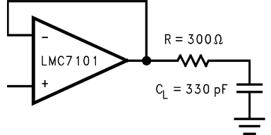
Capacitive load compensation can be accomplished using resistive isolation as shown in Figure 64. This simple technique is useful for isolating the capacitive input of multiplexers and A/D converters.
 Figure 64. Resistive Isolation
of a 330-pF Capacitive Load
8.1.3 Compensating for Input Capacitance When Using Large Value Feedback Resistors
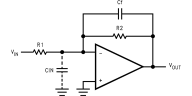
When using very large value feedback resistors, (usually > 500 kΩ) the large feed back resistance can react with the input capacitance due to transducers, photo diodes, and circuit board parasitics to reduce phase margins.
The effect of input capacitance can be compensated for by adding a feedback capacitor. The feedback capacitor (as in Figure 65), Cf is first estimated by Equation 1 and Equation 2, which typically provides significant overcompensation.

Printed circuit board stray capacitance may be larger or smaller than that of a breadboard, so the actual optimum value for CF may be different. The values of CF must be checked on the actual circuit (refer to CMOS Quad Operational Amplifier (SNOSBZ3) for a more detailed discussion).
 Figure 65. Cancelling the Effect of Input Capacitance
8.2 Typical Application
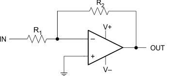
Figure 66 shows a high input impedance noninverting circuit. This circuit gives a closed-loop gain equal to the ratio of the sum of R1 and R2 to R1 and a closed-loop 3-dB bandwidth equal to the amplifier unity-gain frequency divided by the closed-loop gain. This design has the benefit of a very high input impedance, which is equal to the differential input impedance multiplied by loop gain. (Open loop gain/Closed loop gain.) In DC coupled applications, input impedance is not as important as input current and its voltage drop across the source resistance. The amplifier output will go into saturation if the input is allowed to float, which may be important if the amplifier must be switched from source to source.
 Figure 66. Example Application
8.2.1 Design Requirements
For this example application, the supply voltage is 5 V, and 100 × ±5% of noninverting gain is necessary. The signal input impedance is approximately 10 kΩ.
8.2.2 Detailed Design Procedure
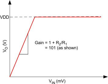
Use the equation for a noninverting amplifier configuration; G = 1 + R2 / R1, set R1 to 10 kΩ, and R2 to 99 × the value of R1, which would be 990 kΩ. Replacing the 990-kΩ resistor with a more readily available 1-MΩ resistor will result in a gain of 101, which is within the desired gain tolerance. The gain-frequency characteristic of the amplifier and its feedback network must be such that oscillation does not occur. To meet this condition, the phase shift through amplifier and feedback network must never exceed 180° for any frequency where the gain of the amplifier and its feedback network is greater than unity. In practical applications, the phase shift must not approach 180° because this is the situation of conditional stability. The most critical case occurs when the attenuation of the feedback network is zero.
8.2.3 Application Curve
 Figure 67. Output Response