SNOS719G September 1999 – September 2015 LMC7101 , LMC7101Q-Q1
PRODUCTION DATA.
- 1 Features
- 2 Applications
- 3 Description
- 4 Revision History
- 5 Pin Configuration and Functions
-
6 Specifications
- 6.1 Absolute Maximum Ratings
- 6.2 ESD Ratings: LMC7101
- 6.3 ESD Ratings: LMC7101Q-Q1
- 6.4 Recommended Operating Conditions
- 6.5 Thermal Information
- 6.6 Electrical Characteristics: 2.7 V
- 6.7 DC Electrical Characteristics: 3 V
- 6.8 DC Electrical Characteristics: 5 V
- 6.9 DC Electrical Characteristics: 15 V
- 6.10 AC Electrical Characteristics: 5 V
- 6.11 AC Electrical Characteristics: 15 V
- 6.12 Typical Characteristics
- 7 Detailed Description
- 8 Application and Implementation
- 9 Power Supply Recommendations
- 10Layout
- 11Device and Documentation Support
- 12Mechanical, Packaging, and Orderable Information
10 Layout
10.1 Layout Guidelines
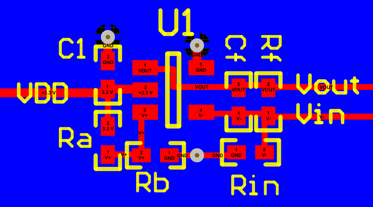
Care must be taken to minimize the loop area formed by the bypass capacitor connection between supply pins and ground. A ground plane underneath the device is recommended; any bypass components to ground must have a nearby via to the ground plane. The optimum bypass capacitor placement is closest to the corresponding supply pin. Use of thicker traces from the bypass capacitors to the corresponding supply pins will lower the power-supply inductance and provide a more stable power supply.
The feedback components must be placed as close as possible to the device to minimize stray parasitics.
10.2 Layout Example
 Figure 68. LMC7101 Example Layout