JAJSLK5B October   2020  – May 2022 LMG3422R050 , LMG3425R050

PRODUCTION DATA  

  1. 特長
  2. アプリケーション
  3. 概要
  4. Revision History
  5. Device Comparison
  6. Pin Configuration and Functions
  7. Specifications
    1. 7.1 Absolute Maximum Ratings
    2. 7.2 ESD Ratings
    3. 7.3 Recommended Operating Conditions
    4. 7.4 Thermal Information
    5. 7.5 Electrical Characteristics
    6. 7.6 Switching Characteristics
    7. 7.7 Typical Characteristics
  8. Parameter Measurement Information
    1. 8.1 Switching Parameters
      1. 8.1.1 Turn-On Times
      2. 8.1.2 Turn-Off Times
      3. 8.1.3 Drain-Source Turn-On Slew Rate
      4. 8.1.4 Turn-On and Turn-Off Switching Energy
  9. Detailed Description
    1. 9.1 Overview
    2. 9.2 Functional Block Diagram
    3. 9.3 Feature Description
      1. 9.3.1  GaN FET Operation Definitions
      2. 9.3.2  Direct-Drive GaN Architecture
      3. 9.3.3  Drain-Source Voltage Capability
      4. 9.3.4  Internal Buck-Boost DC-DC Converter
      5. 9.3.5  VDD Bias Supply
      6. 9.3.6  Auxiliary LDO
      7. 9.3.7  Fault Detection
        1. 9.3.7.1 Overcurrent Protection and Short-Circuit Protection
        2. 9.3.7.2 Overtemperature Shutdown
        3. 9.3.7.3 UVLO Protection
        4. 9.3.7.4 Fault Reporting
      8. 9.3.8  Drive Strength Adjustment
      9. 9.3.9  Temperature-Sensing Output
      10. 9.3.10 Ideal-Diode Mode Operation
    4. 9.4 Start Up Sequence
    5. 9.5 Safe Operation Area (SOA)
      1. 9.5.1 Safe Operation Area (SOA) - Repetitive SOA
    6. 9.6 Device Functional Modes
  10. 10Application and Implementation
    1. 10.1 Application Information
    2. 10.2 Typical Application
      1. 10.2.1 Design Requirements
      2. 10.2.2 Detailed Design Procedure
        1. 10.2.2.1 Slew Rate Selection
          1. 10.2.2.1.1 Start-Up and Slew Rate With Bootstrap High-Side Supply
        2. 10.2.2.2 Signal Level-Shifting
        3. 10.2.2.3 Buck-Boost Converter Design
      3. 10.2.3 Application Curves
    3. 10.3 Do's and Don'ts
  11. 11Power Supply Recommendations
    1. 11.1 Using an Isolated Power Supply
    2. 11.2 Using a Bootstrap Diode
      1. 11.2.1 Diode Selection
      2. 11.2.2 Managing the Bootstrap Voltage
  12. 12Layout
    1. 12.1 Layout Guidelines
      1. 12.1.1 Solder-Joint Reliability
      2. 12.1.2 Power-Loop Inductance
      3. 12.1.3 Signal-Ground Connection
      4. 12.1.4 Bypass Capacitors
      5. 12.1.5 Switch-Node Capacitance
      6. 12.1.6 Signal Integrity
      7. 12.1.7 High-Voltage Spacing
      8. 12.1.8 Thermal Recommendations
    2. 12.2 Layout Examples
  13. 13Device and Documentation Support
    1. 13.1 Documentation Support
      1. 13.1.1 Related Documentation
    2. 13.2 Receiving Notification of Documentation Updates
    3. 13.3 サポート・リソース
    4. 13.4 Trademarks
    5. 13.5 Electrostatic Discharge Caution
    6. 13.6 Export Control Notice
    7. 13.7 Glossary
  14. 14Mechanical, Packaging, and Orderable Information

パッケージ・オプション

メカニカル・データ(パッケージ|ピン)
  • RQZ|54
サーマルパッド・メカニカル・データ
発注情報

Layout Examples

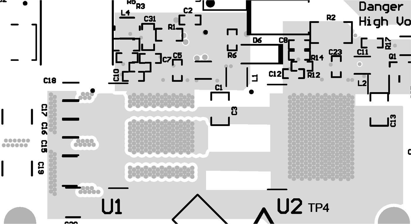
Correct layout of the LMG342xR050 and its surrounding components is essential for correct operation. The layouts shown here reflect the GaN device schematic in Figure 10-1. These layouts are shown to produce good results and is intended as a guideline. However, it can be possible to obtain acceptable performance with alternate layout schemes. Additionally, please refer to the land pattern example in Mechanical, Packaging, and Orderable Information for the latest recommended PCB footprint of the device.

The the top-layer layout and mid-layer layout are shown. The layouts are zoomed in to the LMG342xR050 U1 and U2 component placements. The mid-layer layout includes the outlines of the top level components to assist the reader in lining up the top-layer and mid-layer layouts.
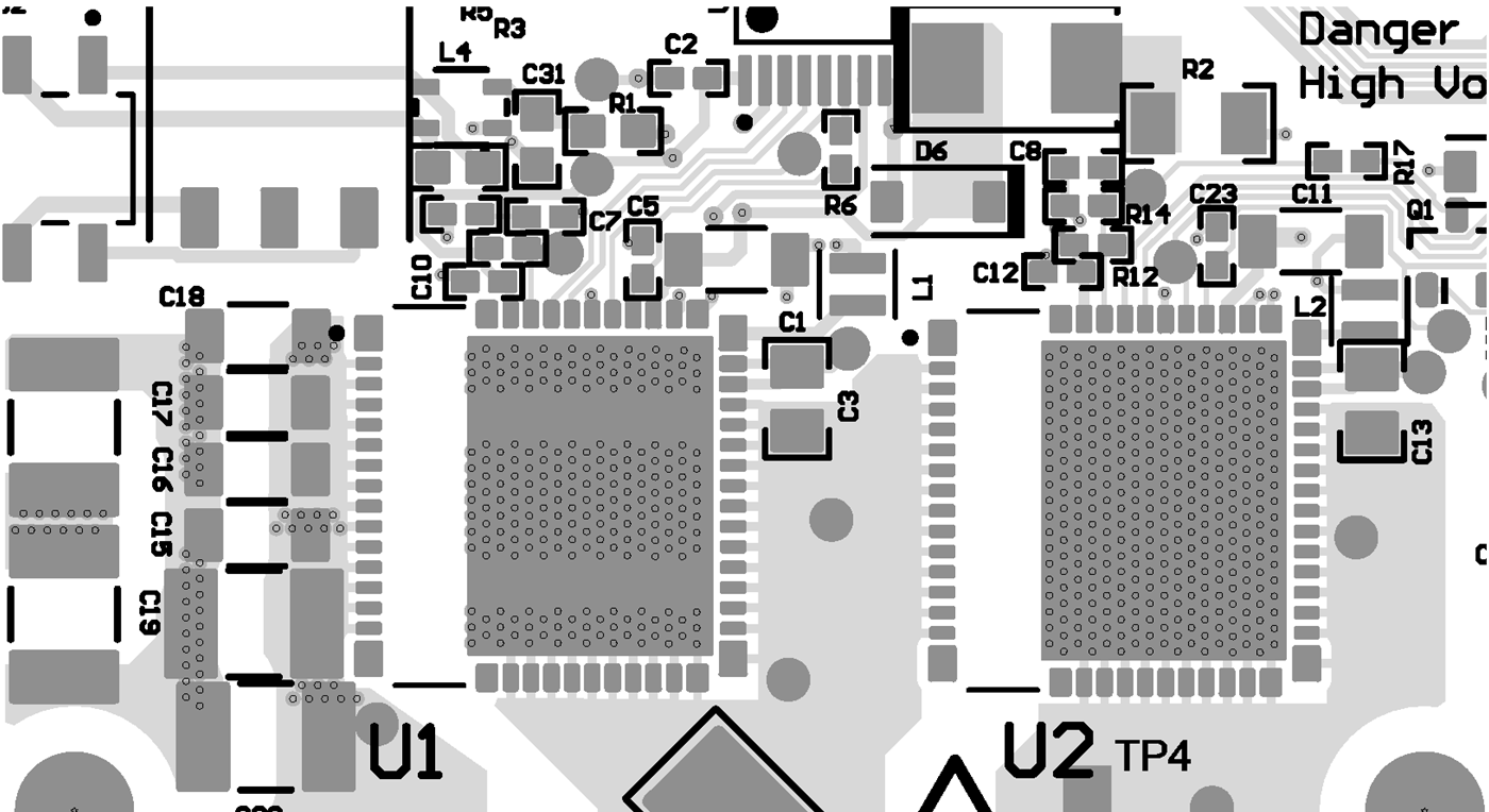
GUID-20211130-SS0I-C5LF-MJKT-K65LJJBRVRKV-low.png Figure 12-1 Half-Bridge Top-Layer Layout
GUID-20211130-SS0I-WF2V-GQV0-1B61GHRWJ8S2-low.png Figure 12-2 Half-Bridge Mid-Layer Layout