JAJSFM3E February   2015  – June 2018 LMH1218

PRODUCTION DATA.  

  1. 特長
  2. アプリケーション
  3. 概要
    1.     Device Images
      1.      SPI概略回路図
  4. 改訂履歴
  5. 概要(続き)
  6. Pin Configuration and Functions
    1.     Pin Descriptions – SPI Mode/ Mode_SEL = 1 kΩ to VDD
    2.     Pin Descriptions – SMBUS Mode/ MODE_SEL = 1 kΩ to GND
  7. Specifications
    1. 7.1 Absolute Maximum Ratings
    2. 7.2 ESD Ratings
    3. 7.3 Recommended Operating Conditions
    4. 7.4 Thermal Information
    5. 7.5 Electrical Characteristics
    6. 7.6 Recommended SMBus Interface AC Timing Specifications
    7. 7.7 Serial Parallel Interface (SPI) Bus Interface AC Timing Specifications
    8. 7.8 Typical Characteristics
  8. Detailed Description
    1. 8.1 Overview
    2. 8.2 Functional Block Diagram
    3. 8.3 Feature Description
      1. 8.3.1 Loss of Signal Detector
      2. 8.3.2 Continuous Time Linear Equalizer (CTLE)
      3. 8.3.3 2:1 Multiplexer
      4. 8.3.4 Clock and Data Recovery
      5. 8.3.5 Eye Opening Monitor (EOM)
      6. 8.3.6 Fast EOM
        1. 8.3.6.1 SMBus Fast EOM Operation
        2. 8.3.6.2 SPI Fast EOM Operation
      7. 8.3.7 LMH1218 Device Configuration
        1. 8.3.7.1 MODE_SEL
        2. 8.3.7.2 ENABLE
        3. 8.3.7.3 LOS_INT_N
        4. 8.3.7.4 LOCK
        5. 8.3.7.5 SMBus MODE
        6. 8.3.7.6 SMBus READ/WRITE Transaction
        7. 8.3.7.7 SPI Mode
          1. 8.3.7.7.1 SPI READ/WRITE Transaction
          2. 8.3.7.7.2 SPI Write Transaction Format
          3. 8.3.7.7.3 SPI Read Transaction Format
        8. 8.3.7.8 SPI Daisy Chain
          1. 8.3.7.8.1 SPI Daisy Chain Write Example
          2. 8.3.7.8.2 SPI Daisy Chain Write Read Example
            1. 8.3.7.8.2.1 SPI Daisy Chain Length of Daisy Chain Illustration
      8. 8.3.8 Power-On Reset
    4. 8.4 Device Functional Modes
    5. 8.5 Programming
    6. 8.6 Register Maps
      1. 8.6.1 Global Registers
      2. 8.6.2 Receiver Registers
      3. 8.6.3 CDR Registers
      4. 8.6.4 Transmitter Registers
  9. Application and Implementation
    1. 9.1 Application Information
      1. 9.1.1 General Guidance for All Applications
    2. 9.2 Typical Application
      1. 9.2.1 Design Requirements
      2. 9.2.2 Detailed Design Procedure
      3. 9.2.3 Application Curves
    3. 9.3 Do's and Don'ts
    4. 9.4 Initialization Set Up
      1. 9.4.1 Selective Data Rate Lock
  10. 10Power Supply Recommendations
  11. 11Layout
    1. 11.1 Layout Guidelines
    2. 11.2 Layout Example
    3. 11.3 Solder Profile
  12. 12デバイスおよびドキュメントのサポート
    1. 12.1 デバイス・サポート
      1. 12.1.1 開発サポート
    2. 12.2 ドキュメントのサポート
      1. 12.2.1 関連資料
    3. 12.3 ドキュメントの更新通知を受け取る方法
    4. 12.4 コミュニティ・リソース
    5. 12.5 商標
    6. 12.6 静電気放電に関する注意事項
    7. 12.7 Glossary
  13. 13メカニカル、パッケージ、および注文情報

パッケージ・オプション

メカニカル・データ(パッケージ|ピン)
サーマルパッド・メカニカル・データ
発注情報

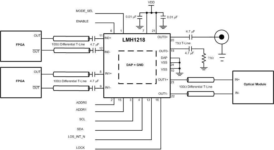
Design Requirements

For the LMH1218 design example, the requirements noted in Table 9 apply.

Table 9. LMH1218 Design Parameters

DESIGN PARAMETER REQUIREMENT
Input AC coupling capacitors Required. 4.7 µF AC coupling capacitors are recommended. Capacitors may be implemented on the PCB or in the connector.
Output AC coupling capacitors Required. Both OUT0 and OUT1 require AC coupling capacitors. OUT0 AC Coupling capacitors is expected to be 4.7 µF to comply with SMPTE wander requirement. It is assumed that Optical Module has AC coupling capacitors on its input within the module
DC Power Supply Coupling Capacitors To minimize power supply noise, use 0.01 µF capacitors as close to the device VDD pins as possible
Distance from Device to BNC Keep this distance within 1 inch to meet Proposed ST-2081 and ST-2082 requirements
High Speed IN0, IN1, OUT0, and OUT1 trace impedance Design differential trace impedance of IN0, IN1, and OUT1 with 100-Ω ± 5%, single-end trace impedance for OUT0 with 75 Ω ± 5%
LMH1218 smbus_mode_config_snls474.gifFigure 24. LMH1218 SMBus Mode Configuration