JAJSA84E February 2005 – May 2016 LMH6703
PRODUCTION DATA.
- 1 特長
- 2 アプリケーション
- 3 概要
- 4 改訂履歴
- 5 Pin Configuration and Functions
- 6 Specifications
- 7 Typical Characteristics
- 8 Detailed Description
- 9 Application and Implementation
- 10Power Supply Recommendations
- 11Layout
- 12デバイスおよびドキュメントのサポート
- 13メカニカル、パッケージ、および注文情報
パッケージ・オプション
メカニカル・データ(パッケージ|ピン)
サーマルパッド・メカニカル・データ
発注情報
8 Detailed Description
8.1 Overview
The LMH6703 has been optimized for exceptionally low harmonic distortion while driving very demanding resistive or capacitive loads. Generally, when used as the input amplifier to very high speed flash ADCs, the distortions introduced by the converter will dominate over the low LMH6703 distortions shown in Typical Characteristics.
8.2 Feature Description
The LMH6703 is a high speed current feedback amplifier, optimized for excellent bandwidth, gain flatness, and low distortion. The loop gain for a current feedback op amp, and hence the frequency response, is predominantly set by the feedback resistor value. The LMH6703 in the SOT-23-6 package is optimized for use with a 560-Ω feedback resistor. The LMH6703 in the SOIC package is optimized for use with a 390-Ω feedback resistor. Using lower values can lead to excessive ringing in the pulse response while a higher value will limit the bandwidth. Application Note OA-13 (SNOA366) discusses this in detail along with the occasions where a different RF might be advantageous.
8.3 Device Functional Modes
8.3.1 Feedback Resistor Selection
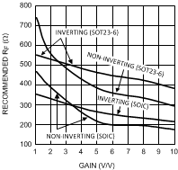
One of the key benefits of a current feedback operational amplifier is the ability to maintain optimum frequency response independent of gain by using appropriate values for the feedback resistor (RF). The Electrical Characteristics and Typical Characteristics plots specify an RF of 560 Ω (390 Ω for the SOIC package), a gain of 2 V/V, and ±5-V power supplies (unless otherwise specified). Generally, lowering RF from it’s recommended value will peak the frequency response and extend the bandwidth while increasing the value of RF will cause the frequency response to roll off faster. Reducing the value of RF too far below it’s recommended value will cause overshoot, ringing and, eventually, oscillation.
 Figure 27. Recommended RF vs. Gain
Since a current feedback amplifier is dependant on the value of RF to provide frequency compensation and since the value of RF can be used to optimize the frequency response, different packages use different RF values. As shown in Figure 27, the SOT-23-6 and the SOIC package use different values for the feedback resistor, RF. Since each application is slightly different, it is worth some experimentation to find the optimal RF for a given circuit. In general, a value of RF that produces ≈0.1 dB of peaking is the best compromise between stability and maximum bandwidth. Note that it is not possible to use a current feedback amplifier with the output shorted directly to the inverting input. The buffer configuration of the LMH6703 requires a 560 Ω (390 Ω for SOIC package) feedback resistor for stable operation.
The LMH6703 was optimized for high speed operation. As shown in Figure 27, the suggested value for RF decreases for higher gains. Due to the output impedance of the input buffer, there is a practical limit for how small RF can go, based on the lowest practical value of RG. This limitation applies to both inverting and non inverting configurations. For the LMH6703 the input resistance of the inverting input is approximately 30Ω and 20Ω is a practical (but not hard and fast) lower limit for RG. The LMH6703 begins to operate in a gain bandwidth limited fashion in the region when RG is nearly equal to the input buffer impedance. Note that the amplifier will operate with RG values well below 20 Ω, however results may be substantially different than predicted from ideal models. In particular the voltage potential between the Inverting and Non-Inverting inputs cannot be expected to remain small.
Inverting gain applications that require impedance matched inputs may limit gain flexibility somewhat (especially if maximum bandwidth is required). The impedance seen by the source is RG || RT (RT is optional). The value of RG is RF /Gain. Thus for a SOT-23 in a gain of —5V/V, an RF of 460 Ω is optimum and RG is 92 Ω. Without a termination resistor, RT, the input impedance would equal RG, 92 Ω. Using an RT of 109Ω will set the input resistance to match a 50-Ω source. Note that source impedances greater then RG cannot be matched in the inverting configuration.
For more information see Application Note OA-13 (SNOA366) which describes the relationship between RF and closed-loop frequency response for current feedback operational amplifiers. The value for the inverting input impedance for the LMH6703 is approximately 30 Ω. The LMH6703 is designed for optimum performance at gains of 1 to 10 V/V and −1 to −9 V/V. Higher gain configurations are still useful, however, the bandwidth will fall as gain is increased, much like a typical voltage feedback amplifier.
The LMH6703 data sheet shows both SOT-23-6 and SOIC data in the Electrical Characteristic section to aid in selecting the right package. The Typical Characteristics section shows SOT-23-6 package plots only.
8.3.2 DC Accuracy and Noise
Example below shows the output offset computation equation for the non-inverting configuration (see Figure 29) using the typical bias current and offset specifications for AV = 2:
Output Offset : VO = (IBN × RIN ± VOS) (1 + RF/RG) ± IBI × RF
Where RIN is the equivalent input impedance on the non-inverting input.
Example computation for AV = 2, RF = 560 Ω, RIN = 25 Ω:
VO = (7 μA × 25 Ω ± 1.5 mV) (1 + 560/560) ± 2 μA × 560≈ −3.7 mV to 4.5 mV
A good design, however, should include a worst case calculation using Min/Max numbers in the data sheet tables, in order to ensure "worst case" operation.
Further improvement in the output offset voltage and drift is possible using the composite amplifiers described in Application Note OA-07 (SNOA365). The two input bias currents are physically unrelated in both magnitude and polarity for the current feedback topology. It is not possible, therefore, to cancel their effects by matching the source impedance for the two inputs (as is commonly done for matched input bias current devices).
The total output noise is computed in a similar fashion to the output offset voltage. Using the input noise voltage and the two input noise currents, the output noise is developed through the same gain equations for each term but combined as the square root of the sum of squared contributing elements. See Application Note OA-12 (SNOA375) for a full discussion of noise calculations for current feedback amplifiers.
8.3.3 Enable/Disable
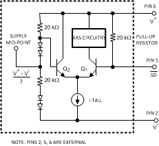
 Figure 28. SD Pin Simplified Schematic
(SOT-23 Pinout Shown)
For 5-V supplies only, the LMH6703 has a TTL logic compatible disable function. Apply a logic low (< 0.8 V) to the SD pin and the LMH6703 is disabled. Apply a logic high (> 2.0 V), or let the pin float and the LMH6703 is enabled. Voltage, not current, at the Shutdown pin (SD) determines the enable/disable state. Care must be exercised to prevent the shutdown pin voltage from going more than 0.8 V below the midpoint of the supply voltages (0V with split supplies, V+/2 with single supply biasing). Doing so could cause transistor Q1 to Zener resulting in damage to the disable circuit (See Figure 28). The core amplifier is unaffected by this, but the shutdown operation could become permanently slower as a result.
Disabled, the LMH6703 inputs and output become high impedances. While disabled the LMH6703 quiescent current is approximately 200 µA. Because of the pull up resistor on the shutdown circuit, the ICC and IEE currents (positive and negative supply currents respectively) are not balanced in the disabled state. The positive supply current (ICC) is approximately 300 µA while the negative supply current (IEE) is only 200 µA. The remaining IEE current of 100 µA flows through the shutdown pin.
The disable function can be used to create analog switches or multiplexers. Implement a single analog switch with one LMH6703 positioned between an input and output. Create an analog multiplexer with several LMH6703s and tie the outputs together.