JAJSHL8B June 2012 – June 2019 LMR12015 , LMR12020
PRODUCTION DATA.
- 1 特長
- 2 アプリケーション
- 3 概要
- 4 改訂履歴
- 5 Pin Configuration and Functions
- 6 Specifications
- 7 Detailed Description
-
8 Application and Implementation
- 8.1 Application Information
- 8.2
Typical Application
- 8.2.1
Detailed Design Procedure
- 8.2.1.1 Custom Design With WEBENCH® Tools
- 8.2.1.2 Inductor Selection
- 8.2.1.3 Input Capacitor
- 8.2.1.4 Output Capacitor
- 8.2.1.5 Catch Diode
- 8.2.1.6 Boost Diode (Optional)
- 8.2.1.7 Boost Capacitor
- 8.2.1.8 Output Voltage
- 8.2.1.9 Feedforward Capacitor (Optional)
- 8.2.1.10
Calculating Efficiency and Junction Temperature
- 8.2.1.10.1 Schottky Diode Conduction Losses
- 8.2.1.10.2 Inductor Conduction Losses
- 8.2.1.10.3 MOSFET Conduction Losses
- 8.2.1.10.4 MOSFET Switching Losses
- 8.2.1.10.5 IC Quiescent Losses
- 8.2.1.10.6 MOSFET Driver Losses
- 8.2.1.10.7 Total Power Losses
- 8.2.1.10.8 Efficiency Calculation Example
- 8.2.1.10.9 Calculating the LMR2015/20 Junction Temperature
- 8.2.2 Application Curves
- 8.2.3 LMR12015/20 Circuit Examples
- 8.2.1
Detailed Design Procedure
- 9 Layout
- 10デバイスおよびドキュメントのサポート
- 11メカニカル、パッケージ、および注文情報
パッケージ・オプション
メカニカル・データ(パッケージ|ピン)
- DSC|10
サーマルパッド・メカニカル・データ
- DSC|10
発注情報
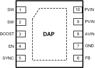
5 Pin Configuration and Functions
DSC Package
10-Pin WSON
Top View

Pin Descriptions
| PIN | DESCRIPTION | |
|---|---|---|
| NO. | NAME | |
| 1,2 | SW | Output switch. Connects to the inductor, catch diode, and bootstrap capacitor. |
| 3 | BOOST | Boost voltage that drives the internal NMOS control switch. A bootstrap capacitor is connected between the BOOST and SW pins. |
| 4 | EN | Enable control input. Logic high enables operation. Do not allow this pin to float or be greater than VIN + 0.3 V. |
| 5 | SYNC | Frequency synchronization input. Drive this pin with an external clock or pulse train. Ground it to use the internal clock. |
| 6 | FB | Feedback pin. Connect FB to the external resistor divider to set output voltage. |
| 7 | GND | Signal and Power Ground pin. Place the bottom resistor of the feedback network as close as possible to this pin for accurate regulation. |
| 8 | AVIN | Supply voltage for the control circuitry. |
| 9,10 | PVIN | Supply voltage for output power stage. Connect a bypass capacitor to this pin. |
| DAP | GND | Signal / Power Ground and thermal connection. Tie this directly to GND (pin 7). See regarding optimum thermal layout. |