JAJSI49C October   2019  – November 2020 LMR33640

PRODUCTION DATA  

  1. 特長
  2. アプリケーション
  3. 概要
  4. Revision History
  5. Device Comparison Table
  6. Pin Configuration and Functions
  7. Specifications
    1. 7.1 Absolute Maximum Ratings
    2. 7.2 ESD Ratings
    3. 7.3 Recommended Operating Conditions
    4. 7.4 Thermal Information
    5. 7.5 Electrical Characteristics
    6. 7.6 Timing Characteristics
    7. 7.7 System Characteristics
    8. 7.8 Typical Characteristics
  8. Detailed Description
    1. 8.1 Overview
    2. 8.2 Functional Block Diagram
    3. 8.3 Feature Description
      1. 8.3.1 Power-Good Flag Output
      2. 8.3.2 Enable and Start-up
      3. 8.3.3 Current Limit and Short Circuit
      4. 8.3.4 Undervoltage Lockout and Thermal Shutdown
    4. 8.4 Device Functional Modes
      1. 8.4.1 Auto Mode
      2. 8.4.2 Dropout
      3. 8.4.3 Minimum Switch On-Time
  9. Application and Implementation
    1. 9.1 Application Information
    2. 9.2 Typical Application
      1. 9.2.1 Design Requirements
      2. 9.2.2 Detailed Design Procedure
        1. 9.2.2.1  Custom Design With WEBENCH® Tools
        2. 9.2.2.2  Setting the Output Voltage
        3. 9.2.2.3  Inductor Selection
        4. 9.2.2.4  Output Capacitor Selection
        5. 9.2.2.5  Input Capacitor Selection
        6. 9.2.2.6  CBOOT
        7. 9.2.2.7  VCC
        8. 9.2.2.8  CFF Selection
        9. 9.2.2.9  External UVLO
        10. 9.2.2.10 Maximum Ambient Temperature
      3. 9.2.3 Application Curves
    3. 9.3 What to Do and What Not to Do
  10. 10Power Supply Recommendations
  11. 11Layout
    1. 11.1 Layout Guidelines
      1. 11.1.1 Ground and Thermal Considerations
    2. 11.2 Layout Example
  12. 12Device and Documentation Support
    1. 12.1 Device Support
      1. 12.1.1 Development Support
        1. 12.1.1.1 Custom Design With WEBENCH® Tools
    2. 12.2 Documentation Support
      1. 12.2.1 Related Documentation
    3. 12.3 Receiving Notification of Documentation Updates
    4. 12.4 Support Resources
    5. 12.5 Trademarks
    6. 12.6 Electrostatic Discharge Caution
    7. 12.7 Glossary
  13. 13Mechanical, Packaging, and Orderable Information

パッケージ・オプション

メカニカル・データ(パッケージ|ピン)
サーマルパッド・メカニカル・データ
発注情報

Setting the Output Voltage

The output voltage of LMR33640 is externally adjustable using a resistor divider network. The range of recommended output voltage is found in Section 7.5. The divider network is comprised of RFBT and RFBB and closes the loop between the output voltage and the converter. The converter regulates the output voltage by holding the voltage on the FB pin equal to the internal reference voltage, VREF. The resistance of the divider is a compromise between excessive noise pickup and excessive loading of the output. Smaller values of resistance reduce noise sensitivity and reduce the light-load efficiency. The recommended value for RFBT is 100 kΩ with a maximum value of 1 MΩ. If a 1 MΩ is selected for RFBT, then a feedforward capacitor must be used across this resistor to provide adequate loop-phase margin (see the Section 9.2.2.8 section). Once RFBT is selected, use Equation 3 to select RFBB. VREF is nominally 1 V (see Section 7.5 for limits).

Equation 3. GUID-3F3A5C7E-8970-4B7E-8F09-23900280A05B-low.gif

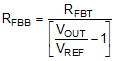
For this 5-V example, RFBT = 100 kΩ and RFBB = 24.9 kΩ are chosen.