JAJSI07A October   2019  – February 2020 LMR36510

PRODUCTION DATA.  

  1. 特長
  2. アプリケーション
  3. 概要
    1.     Device Images
      1.      効率と出力電流との関係 VOUT = 5V、400kHz
      2.      概略回路図
  4. 改訂履歴
  5. Description
  6. Pin Configuration and Functions
    1.     Pin Functions
  7. Specifications
    1. 7.1 Absolute Maximum Ratings
    2. 7.2 ESD Ratings
    3. 7.3 Recommended Operating Conditions
    4. 7.4 Thermal Information
    5. 7.5 Electrical Characteristics
    6. 7.6 Timing Requirements
    7. 7.7 Switching Characteristics
    8. 7.8 System Characteristics
    9. 7.9 Typical Characteristics
  8. Detailed Description
    1. 8.1 Overview
    2. 8.2 Functional Block Diagram
    3. 8.3 Feature Description
      1. 8.3.1 Power-Good Flag Output
      2. 8.3.2 Enable and Start-up
      3. 8.3.3 Current Limit and Short Circuit
      4. 8.3.4 Undervoltage Lockout and Thermal Shutdown
    4. 8.4 Device Functional Modes
      1. 8.4.1 Auto Mode
      2. 8.4.2 Dropout
      3. 8.4.3 Minimum Switch On-Time
  9. Application and Implementation
    1. 9.1 Application Information
    2. 9.2 Typical Application
      1. 9.2.1 Design 1: Low Power 24-V, 1-A Buck Converter
        1. 9.2.1.1 Design Requirements
        2. 9.2.1.2 Detailed Design Procedure
          1. 9.2.1.2.1  Choosing the Switching Frequency
          2. 9.2.1.2.2  Setting the Output Voltage
          3. 9.2.1.2.3  Inductor Selection
          4. 9.2.1.2.4  Output Capacitor Selection
          5. 9.2.1.2.5  Input Capacitor Selection
          6. 9.2.1.2.6  CBOOT
          7. 9.2.1.2.7  VCC
          8. 9.2.1.2.8  CFF Selection
          9. 9.2.1.2.9  External UVLO
          10. 9.2.1.2.10 Maximum Ambient Temperature
      2. 9.2.2 Application Curves
    3. 9.3 What to Do and What Not to Do
  10. 10Power Supply Recommendations
  11. 11Layout
    1. 11.1 Layout Guidelines
      1. 11.1.1 Ground and Thermal Considerations
    2. 11.2 Layout Example
  12. 12デバイスおよびドキュメントのサポート
    1. 12.1 デバイス・サポート
      1. 12.1.1 開発サポート
    2. 12.2 ドキュメントのサポート
      1. 12.2.1 関連資料
    3. 12.3 ドキュメントの更新通知を受け取る方法
    4. 12.4 サポート・リソース
    5. 12.5 商標
    6. 12.6 静電気放電に関する注意事項
    7. 12.7 Glossary
  13. 13メカニカル、パッケージ、および注文情報

パッケージ・オプション

メカニカル・データ(パッケージ|ピン)
サーマルパッド・メカニカル・データ
発注情報

Dropout

The dropout performance of any buck regulator is affected by the RDSON of the power MOSFETs, the DC resistance of the inductor, and the maximum duty cycle that the controller can achieve. As the input voltage is reduced to the output voltage, the off-time of the high-side MOSFET starts to approach the minimum value. Beyond this point, the switching can become erratic and the output voltage falls out of regulation. To avoid this problem, the LMR36510 automatically reduces the switching frequency to increase the effective duty cycle and maintain regulation. In this data sheet, the dropout voltage is defined as the difference between the input and output voltage when the output has dropped by 1% of the nominal value. Under this condition, the switching frequency has dropped to its minimum value of about 140 kHz. Note that the 0.4 V short circuit detection threshold is not activated when in dropout mode.
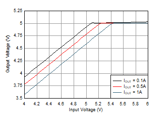
LMR36510 Dropout_LMR36510_5V_22uH.gifFigure 11. Overall Dropout Characteristic
VOUT = 5 V
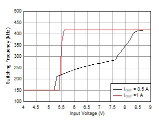
LMR36510 Frequency_Dropout.gifFigure 12. Frequency Dropout Characteristics
ƒSW = 400 kHz