JAJSF93 April   2018 LMV7239-Q1

PRODUCTION DATA.  

  1. 特長
  2. アプリケーション
  3. 概要
    1.     Device Images
      1.      消費電流と電源電圧との関係
      2.      伝搬遅延とオーバードライブ
  4. 改訂履歴
  5. Pin Configuration and Functions
    1.     Pin Functions
  6. Specifications
    1. 6.1 Absolute Maximum Ratings
    2. 6.2 ESD Ratings
    3. 6.3 Recommended Operating Conditions
    4. 6.4 Thermal Information
    5. 6.5 Electrical Characteristics, 2.7 V
    6. 6.6 Electrical Characteristics, 5 V
    7. 6.7 Typical Characteristics
  7. Detailed Description
    1. 7.1 Overview
    2. 7.2 Functional Block Diagram
    3. 7.3 Feature Description
      1. 7.3.1 Input Stage
      2. 7.3.2 Output Stage: LMV7239-Q1
    4. 7.4 Device Functional Modes
      1. 7.4.1 Capacitive and Resistive Loads
      2. 7.4.2 Noise
      3. 7.4.3 Hysteresis
        1. 7.4.3.1 Inverting Comparator With Hysteresis
        2. 7.4.3.2 Non-Inverting Comparator With Hysteresis
      4. 7.4.4 Zero Crossing Detector
        1. 7.4.4.1 Zero Crossing Detector With Hysteresis
      5. 7.4.5 Threshold Detector
  8. Application and Implementation
    1. 8.1 Application Information
    2. 8.2 Typical Applications
      1. 8.2.1 Square Wave Oscillator
        1. 8.2.1.1 Design Requirements
        2. 8.2.1.2 Detailed Design Procedure
        3. 8.2.1.3 Application Curves
      2. 8.2.2 Crystal Oscillator
      3. 8.2.3 Infrared (IR) Receiver
      4. 8.2.4 Window Detector
  9. Power Supply Recommendations
  10. 10Layout
    1. 10.1 Layout Guidelines
    2. 10.2 Layout Example
  11. 11デバイスおよびドキュメントのサポート
    1. 11.1 デバイス・サポート
      1. 11.1.1 開発サポート
    2. 11.2 ドキュメントのサポート
      1. 11.2.1 関連資料
    3. 11.3 ドキュメントの更新通知を受け取る方法
    4. 11.4 コミュニティ・リソース
    5. 11.5 商標
    6. 11.6 静電気放電に関する注意事項
    7. 11.7 Glossary
  12. 12メカニカル、パッケージ、および注文情報

パッケージ・オプション

メカニカル・データ(パッケージ|ピン)
サーマルパッド・メカニカル・データ
発注情報

Non-Inverting Comparator With Hysteresis

A noninverting comparator with hysteresis requires a two resistor network, and a voltage reference (VREF) at the inverting input. When VIN is low, the output is also low. For the output to switch from low to high, VIN must rise up to VIN1 where VIN1 is calculated by:

Equation 4. LMV7239-Q1 eq02_snoscz2.gif

As soon as VO switches to VCC, VA steps to a value greater than VREF which is given by:

Equation 5. LMV7239-Q1 eq03_snoscz2.gif

To make the comparator switch back to its low state, VIN must equal VREF before VA will again equal VREF. VIN2 can be calculated by:

Equation 6. LMV7239-Q1 eq04_snoscz2.gif

The hysteresis of this circuit is the difference between VIN1 and VIN2.

Equation 7. ΔVIN = VCCR1 / R2
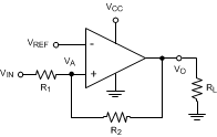
LMV7239-Q1 20201342.gifFigure 19. Noninverting Comparator With Hysteresis
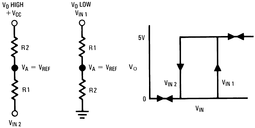
LMV7239-Q1 20201335.pngFigure 20. Noninverting Comparator Thresholds